TIMERS
Presentation
A timer is an hardware counter that can provide accurate timestamps and time-interval measurements.
The L476 microcontroller offers 16 timers:
two 16-bit basic timers (TIM6, TIM7)
two 16-bit advanced motor-control timers (TIM1, TIM8)
five 16-bit general purpose timers (TIM3, TIM4, TIM15, TIM16, TIM17)
two 32-bit general purpose timers (TIM2, TIM5)
two low-power 16-bit timers (LPTIM1, LPTIM2)
two watchdogs
one SysTick timer
There is no TIM9, 10, 11, 12, 13 or 14 in a STM32L476.
Basic timers
Let’s begin with a basic timer. The two basic timers are TIM6 and TIM7. We will use timer6.
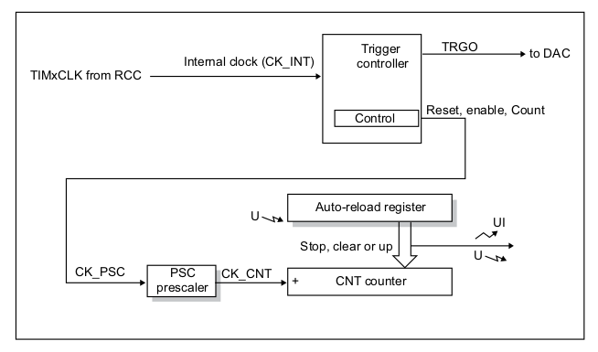
The basic timer is a 16-bit upcounter (TIMx_CNT) with an auto-reload register (TIMx_PSC) and a prescaler register (TIMx_ARR).
TIMx_CNT is a 16-bit register where the current count is stored.
TIMx_ARR contains the 16-bit reload value for the counter.
The counter counts from 0 to the auto-reload value - saved in TIMx_ARR, then restarts from 0 and generates a counter overflow event.
When the counter overflows, it can change an Update Interrupt (UI) or/and an Update (U) flag.
TIMx status register (TIMx_SR)(x = 6 to 7) * Address offset: 0x10

Bit 0 UIF: Update interrupt flag:
0: No update occurred.
1: Update interrupt pending. This bit is set by hardware when the registers are updated:
At overflow or underflow regarding the repetition counter value and if UDIS = 0 in the TIMx_CR1 register.
When CNT is reinitialized by software using the UG bit in the TIMx_EGR register, if URS = 0 and UDIS = 0 in the TIMx_CR1 register.
TIMx event generation register (TIMx_EGR)(x = 6 to 7) * Address offset: 0x14

Bit 0 UG: Update generation:
0: No action.
1: Re-initializes the timer counter and generates an update of the registers.
When the counters cycle is restarted, it fires an “update event” which can be found in the TIM_SR register as the Update Interrupt Flag (UIF). This value needs to be reset to continue receiving notifications.
The counter is clocked by the prescaler output CK_CNT, which is enabled only when the counter enable bit (CEN) in the TIMx_CR1 register is set.
Use a basic timer to generate a delay with polling
To configure and run the STM32L476 basic timer TIM6 without using interrupts, we can use a polling method to check the update flag.
This example will initialize TIM6 to generate a 1-second delay. In this approach, we wait for the UIF (Update Interrupt Flag) bit to be set in the TIM6_SR status register, indicating that the timer has overflowed.
Timer clock enable
First of all, we need to enable the timer clock.
From the block diagram found in the L476 datasheet (page 17/270), we see that TIM6 is connected to the APB1 bus.

So we will enable the TIM6 clock using the bit 4 of the APB1ENR1 register:

1       #define GPIO_MODER_MODE5_Pos  (10U)
2       #define GPIO_MODER_MODE5_Msk  (0x3UL << GPIO_MODER_MODE5_Pos)         /*!< 0x00000C00 */
3
4       #define GPIO_MODER_MODE5      GPIO_MODER_MODE5_Msk
5       #define GPIO_MODER_MODE5_0   (0x1UL << GPIO_MODER_MODE5_Pos)         /*!< 0x00000400  01 00 00 00 00 00 */
6       #define GPIO_MODER_MODE5_1   (0x2UL << GPIO_MODER_MODE5_Pos)         /*!< 0x00000800  10 00 00 00 00 00 */
Registers
register CR1

register SR

This bit is set by hardware when the registers are updated:
At overflow or underflow regarding the repetition counter value and if UDIS = 0 in the TIMx_CR1 register.
When CNT is reinitialized by software using the UG bit in the TIMx_EGR register, if URS = 0 and UDIS = 0 in the TIMx_CR1 register.
Behavior
Let’s consider a basic 16-bit timer. It can count from 0 up to 65535. Every clock cycle, the value of the timer is incremented by 1.
The counter frequency is the system frequency Fsys divided by the value of the Prescaler.
 1       // ----------- enable timer 6 clock ---------------------
 2       ldr r0,=RCC_BASE
 3       ldr r1,[r0,#RCC_APB1ENR1]
 4       orr r1,#(1<<4)      // RCC_APB1ENR1_TIM6EN 0x10 TIM6EN bit 4 - see RM p. 253/1890
 5       str r1,[r0,#RCC_APB1ENR1]
 6
 7       // ------------------ TIMER 6 ------------------
 8       ldr r0,=TIM6_BASE
 9
10       // configure TIM6 prescaler and auto-reload for a 1-second delay
11       //  freq = 4 MHz / ((PSC - 1) * (ARR - 1))
12       ldr r1, =7999     // prescaler to 7999 (80 MHz / (7999 + 1) = 10 kHz)
13       str r1, [r0, #PSC]
14
15       ldr r1, =9999     // auto-reload value for 1-second delay
16       str r1,[r0,#ARR]  // count up to 16 bit max, ie 0xFFFF = 65535
Use a basic timer to generate a delay with interruption
aaa
1111
222222
bbb
General purpose timers
Instead of polling, we can configure the timer to directly toggle an output, for example the User LED.
Compare with output
In order to do this we need to use a more powerful timer, such as a general purpose timer.
Configure PA5 (LED) as alternate function

The table show us that the only available PA5 timer alternate functions are TIM2_CH1 (AF1), TIM2_ETR (AF2), TIM8_CH1N (AF3) and also LPTIM2_ETR (AF14).
We choose TIM2_CH1 (AF1).
We set the alternate mode of the GPIO pin x by setting the bit 1 and resetting the bit 0:
10: Alternate function mode
reset bit 0 with bic
set bit 1 with orr
With PA5:
1 // ----------- set PA5 alternate function
2 ldr r0, =GPIOA_BASE                //  4800 0000
3 ldr r1, [r0,#GPIO_MODER]
4 bic r1, r1, #GPIO_MODER_MODE5_0    // clear bit0 "x0"
5 orr r1, r1, #GPIO_MODER_MODE5_1    //   set bit1 "1x"
6 str r1, [r0,#GPIO_MODER]
For a given AFx, we also need to specify one of these two 32-bit alternate function selection registers:
GPIO alternate function low register (GPIOx_AFRL)
(x = A to I) * GPIOx_AFRL for GPIO pin 0 to 7

GPIO alternate function high register (GPIOx_AFRH)
(x = A to I) * GPIOx_AFRH for GPIO pin 8 to 15

Implement alternate function
GPIO
For GPIOA pin 5, we use AFSEL5[0:3] and write the value corresponding to AF1, that is the binary value 0001 (ie 1 as in AF1):
set bit 0 with orr
clear bit 1 with bic
clear bit 2 with bic
ckear bit 3 with bic
Since the pin number is less than 7, we use the GPIOx_AFRL register
 1#define GPIO_AFRL_AFSEL5_Pos  (20U)
 2#define GPIO_AFRL_AFSEL5_Msk           (0xFUL << GPIO_AFRL_AFSEL5_Pos)         /*!< 0x00F00000 */
 3#define GPIO_AFRL_AFSEL5               GPIO_AFRL_AFSEL5_Msk
 4#define GPIO_AFRL_AFSEL5_0             (0x1UL << GPIO_AFRL_AFSEL5_Pos)         /*!< 0x00100000 */
 5#define GPIO_AFRL_AFSEL5_1             (0x2UL << GPIO_AFRL_AFSEL5_Pos)         /*!< 0x00200000 */
 6#define GPIO_AFRL_AFSEL5_2             (0x4UL << GPIO_AFRL_AFSEL5_Pos)         /*!< 0x00400000 */
 7#define GPIO_AFRL_AFSEL5_3             (0x8UL << GPIO_AFRL_AFSEL5_Pos)         /*!< 0x00800000 */
 8
 9
10// alternate function to TIM2_CH1  AFRL->AFSEL[5]= AF1
11ldr  r1, =GPIOA_BASE   //  4800 0000
12ldr r2,[r1,#AFRL]
13orr r2,r2, #GPIO_AFRH_AFSEL5_0
14bic r2,r2, #GPIO_AFRH_AFSEL5_1
15bic r2,r2, #GPIO_AFRH_AFSEL5_2
16bic r2,r2, #GPIO_AFRH_AFSEL5_3
17str r2,[r1,#AFRL]
Channels
TIM2_CH1 means the channel 1 of TIMER2.
The channels can be used as input (capture mode) or in output (compare mode).

Define a comparison value with CCR register
We want to compare the counter (CNT) value with a specific value (preload value) that we write in one of the capture/compare register (there are at most 4 of them).
TIMx capture/compare register 1 (TIMx_CCR1)(x = 2 to 5) * Address offset: 0x34

32-bit counter for TIM2 and TIM5 16-bit counter for others GP timers
If channel CC1 is configured as output: CCR1 is the value to be loaded in the actual capture/compare 1 register (preload value).
It is loaded permanently if the preload feature is not selected in the TIMx_CCMR1 register (bit OC1PE).
Else the preload value is copied in the active capture/compare register when an update event occurs.
When the counter value is greater or equal to this CCR value, it will drive the appropriate channel.
Configure the output mode
First we configure the channel as an ouput.
TIMx capture/compare mode register 1

TIMx_CCMR1 (x = 2 to 5)
Address offset: 0x18
This is done with the 2-bit field Capture/Compare Selection (CCSx) of the Capture/compare mode register corresponding to the channel x used.
00: CC1 channel is configured as output
We can control the output by either putting a logic 1, putting a logic 0, or toggling its value.
We define the content of OC1M[3:0]. These 4 bits define the behavior of the output reference signal OC1REF from which OC1 and OC1N are derived.
OC1REF is active high whereas OC1 and OC1N active level depends
We choose Output compare 1 mode as OC1M Toggle output:
0011: Toggle - OC1REF toggles when TIMx_CNT=TIMx_CCR1.
Select the output mode. For example, one must write OCxM=011, OCxPE=0, CCxP=0 and CCxE=1 to toggle OCx output pin when CNT matches CCRx,
CCER register
TIMx capture/compare enable register
(TIMx_CCER)(x = 2 to 5)

Address offset: 0x20
The CCER register is set to enable the timer to output on pin TIM2_CH1 which we have configured to be PA5.
// CC1E Enable output
TIM1->CCER |= 1;
Bit 0 CC1E: Capture/Compare 1 output enable.
0: Capture mode disabled / OC1 is not active
1: Capture mode enabled / OC1 signal is output on the corresponding output pin
Start the timer
TIM1->CR1 |= 1;
Several types of counting
Up-counting mode
The basic timer can only upcount from 0 to the autoreload (ARR)value. Whenever the counter value is ARR, it overflows and its value becomes 0.

Down-counting mode
The general purpose timers (and advanced timers) have also a down-counting mode:

This timer counts down from ARR to zero. When it hits 0, it underflows and its value becomes ARR.
Center-aligned mode

This timer upcounts from 0 to ARR, then downcounts from ARR to 0. It generates overflows and underflows.
Direction of counting
The following CR1 register is for a basic timer:
TIMx control register 1 (TIMx_CR1)(x = 2 to 5) Address offset: 0x00
We notice there are more functions for a general purpose CR1 register:

We will use:
00: edge-aligned mode. The counter counts up or down depending on the direction bit (DIR).

0: counter used as upcounter
External trigger
Connect button to external trigger ETR
On the Nucleo L476 board, there is a user button (PC13, blue button).
We would like to internally connect this blue button to a trigger input (ETR, input channel 1 or input channel 2).
But there is no alternate function associated with PC13.

There are no trigger possibilities for AF8 to AF15 for PC13 either.
Instead, we have to configure a GPIO port as an alternate function acting as an input to ETR (External TRigger) or channel 1 or channel 2.

Let’s connect one pole of a switch to PA15 with the following wiring:


With the alternate function AF2, the GPIO PA15 will be internally connected to the TIM2 trigger input ETR.

We use AFSEL15[0:3] and write the value corresponding to AF2, that is the binary value 0010 (ie 2 of AF2):
// set PA15 as alternate function "10"
GPIOA->MODER &= ~GPIO_MODER_MODE15_0;
GPIOA->MODER |=  GPIO_MODER_MODE15_1;

// connect timer2  PA15 -> input ETR timer 2 via alternate function AF2  "0010"
GPIOA->AFR[1] &= ~(GPIO_AFRH_AFSEL15_0);
GPIOA->AFR[1] |=   GPIO_AFRH_AFSEL15_1 ;
GPIOA->AFR[1] &= ~(GPIO_AFRH_AFSEL15_2);
GPIOA->AFR[1] &= ~(GPIO_AFRH_AFSEL15_3);

Minimal C program
Each time the button is pressed, the CNT counter increments. When it reaches the maximum value (ARR), it resets to zero.
select falling edge detection on the external trigger (ETR pin) by writing 1 in external trigger polarity bit (ETP, bit 15)
set the External trigger prescaler by writing ETPS[1:0]=00 (prescaler off).
use the external trigger filter (ETF) to debounce input, with ETF[3:0]=1111 where 8 consecutive events are needed to validate a transition on the button.
enable external clock mode 2 by writing ECE=1 in SMCR register
enable the counter by writing CEN=1 in CR1 register

TIMx slave mode control register (TIMx_SMCR)(x = 2 to 5)

// ----- enable GP timer 2 clock ----------
RCC->APB1ENR1 |= RCC_APB1ENR1_TIM2EN;

// ********* TIMER 2 mode and configuration **********
// ETR is inverted, active at low level or falling edge
TIM2->SMCR |= TIM_SMCR_ETP; // External trigger polarity

TIM2->SMCR &= ~TIM_SMCR_ETPS_Msk; // prescaler OFF

TIM2->SMCR |=  TIM_SMCR_ETF_0;  // debounce filter at maximum
TIM2->SMCR |=  TIM_SMCR_ETF_1;
TIM2->SMCR |=  TIM_SMCR_ETF_2;
TIM2->SMCR |=  TIM_SMCR_ETF_3;

TIM2->PSC =  0;   // prescaler OFF
TIM2->ARR =  8;   // maximum number of presses

TIM2->SMCR |=  TIM_SMCR_ECE; // enables external clock Mode 2
TIM2->CR1 |= TIM_CR1_CEN;    // activates timer
When clicking on the button, you should see the CNT counter increments at each click and go back to zero at the 8th press.
With timer 1, button connected to PA12 - TIM_ETR
// set PA12 as alternate function "10"
GPIOA->MODER &= ~GPIO_MODER_MODE12_0;
GPIOA->MODER |=  GPIO_MODER_MODE12_1;

// connect PA12 -> input ETR timer 1 via alternate function AF1
GPIOA->AFR[1] |=   GPIO_AFRH_AFSEL12_0 ;
GPIOA->AFR[1] &= ~(GPIO_AFRH_AFSEL12_1);
GPIOA->AFR[1] &= ~(GPIO_AFRH_AFSEL12_2);
GPIOA->AFR[1] &= ~(GPIO_AFRH_AFSEL12_3);

// ----- enable timer 1 clock ----------
RCC->APB2ENR |= RCC_APB2ENR_TIM1EN;

// ********* TIMER 1 mode and configuration **********
// ETR is inverted, active at low level or falling edge
TIM1->SMCR |= TIM_SMCR_ETP; // External trigger polarity

TIM1->SMCR &= ~TIM_SMCR_ETPS_Msk; // prescaler OFF

TIM1->SMCR |=  TIM_SMCR_ETF_0;  // debounce filter at maximum
TIM1->SMCR |=  TIM_SMCR_ETF_1;
TIM1->SMCR |=  TIM_SMCR_ETF_2;
TIM1->SMCR |=  TIM_SMCR_ETF_3;

TIM1->PSC =  0;   // prescaler OFF
TIM1->ARR =  8;   // maximum number of presses

TIM1->SMCR |= TIM_SMCR_ECE; // enables external clock Mode 2

// TIM1->BDTR |= TIM_BDTR_MOE;   // Main Output Enable

TIM1->CR1 |= TIM_CR1_CEN;    // activates timer
Note
With a button connected to ground, don’t forget to pull up the port of the GPIO
// pull-up value "01"
GPIOA->PUPDR |=  GPIO_PUPDR_PUPD12_0;
GPIOA->PUPDR &= ~GPIO_PUPDR_PUPD12_1;
If the button is connected to +Vcc (through a resistor), pull down the port (write “10”).
With timer 3, button connected to PD2 - TIM_ETR
// set PD2 as alternate function "10"
GPIOD->MODER &= ~GPIO_MODER_MODE2_0;
GPIOD->MODER |=  GPIO_MODER_MODE2_1;

// pull-up 01
GPIOD->PUPDR |=  GPIO_PUPDR_PUPD2_0;
GPIOD->PUPDR &= ~GPIO_PUPDR_PUPD2_1;

// connect timer3  PD2-> input ETR timer 3 via alternate function AF2  "0010"
GPIOD->AFR[0] &= ~(GPIO_AFRL_AFSEL2_0);
GPIOD->AFR[0] |=   GPIO_AFRL_AFSEL2_1 ;
GPIOD->AFR[0] &= ~(GPIO_AFRL_AFSEL2_2);
GPIOD->AFR[0] &= ~(GPIO_AFRL_AFSEL2_3);

// -------------------------------------------------------------
RCC->APB1ENR1 |= RCC_APB1ENR1_TIM3EN;

// ********* TIMER 3 mode and configuration **********
// ETR is inverted, active at low level or falling edge
TIM3->SMCR |= TIM_SMCR_ETP; // External trigger polarity

TIM3->SMCR &= ~TIM_SMCR_ETPS_Msk; // prescaler OFF

TIM3->SMCR |=  TIM_SMCR_ETF_0;  // debounce filter at maximum
TIM3->SMCR |=  TIM_SMCR_ETF_1;
TIM3->SMCR |=  TIM_SMCR_ETF_2;
TIM3->SMCR |=  TIM_SMCR_ETF_3;

TIM3->PSC =  0;   // prescaler OFF
TIM3->ARR =  8;   // maximum number of presses

TIM3->SMCR |= TIM_SMCR_ECE; // enables external clock Mode 2
TIM3->CR1 |= TIM_CR1_CEN;    // activates timer
You can replace
TIMx->SMCR |= TIM_SMCR_ECE; // enables External clock Mode 2
by
// external clock mode 1 with TRGI
// connected to ETRF (SMS=0111 and TS=111).

// SMS slave mode selection
// 0111: External clock source mode 1
TIMx->SMCR |=  TIM_SMCR_SMS_0;
TIMx->SMCR |=  TIM_SMCR_SMS_1;
TIMx->SMCR |=  TIM_SMCR_SMS_2;
TIMx->SMCR &= ~TIM_SMCR_SMS_3;

// select input for triggering
// 111: External Trigger input (ETRF)
TIMx->SMCR |= TIM_SMCR_TS_0;
TIMx->SMCR |= TIM_SMCR_TS_1;
TIMx->SMCR |= TIM_SMCR_TS_2;
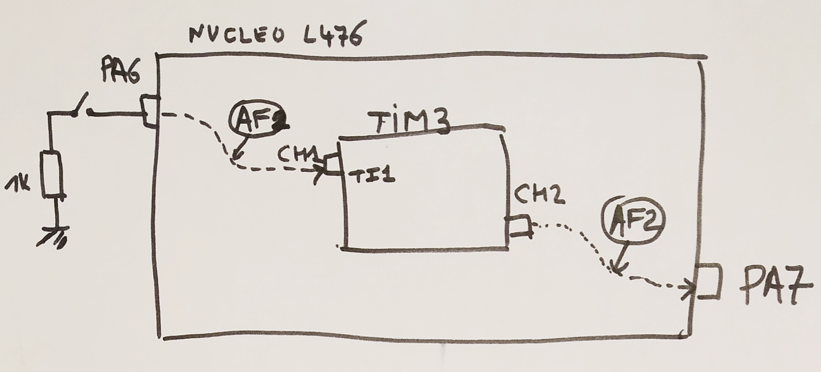
Connect button to external trigger input TI1
The schematics is as below:
// set PA6 as alternate function "10"
GPIOA->MODER &= ~GPIO_MODER_MODE6_0;
GPIOA->MODER |=  GPIO_MODER_MODE6_1;
// pull-up 01
GPIOA->PUPDR |=  GPIO_PUPDR_PUPD6_0;
GPIOA->PUPDR &= ~GPIO_PUPDR_PUPD6_1;

// connect PA6 -> output TIM3 channel 1 via alternate function AF2
GPIOA->AFR[0] &= ~(GPIO_AFRL_AFSEL6_0);
GPIOA->AFR[0] |=   GPIO_AFRL_AFSEL6_1 ;
GPIOA->AFR[0] &= ~(GPIO_AFRL_AFSEL6_2);
GPIOA->AFR[0] &= ~(GPIO_AFRL_AFSEL6_3);

// set PA7 as alternate function "10"
GPIOA->MODER &= ~GPIO_MODER_MODE7_0;
GPIOA->MODER |=  GPIO_MODER_MODE7_1;

// connect PA7 -> output TIM3 channel 2 via alternate function AF2
GPIOA->AFR[0] &= ~(GPIO_AFRL_AFSEL7_0);
GPIOA->AFR[0] |=   GPIO_AFRL_AFSEL7_1 ;
GPIOA->AFR[0] &= ~(GPIO_AFRL_AFSEL7_2);
GPIOA->AFR[0] &= ~(GPIO_AFRL_AFSEL7_3);

// ------------------------------------------------------------------
// ------------------------------------------------------------------
TIM3->PSC =  0;   // prescaler OFF
TIM3->ARR =  5;   // maximum count

TIM3->CCER |= TIM_CCER_CC1P;  // TI1 active low

// 01: CC1 channel is configured as input, IC1 is mapped on TI1
TIM3->CCMR1 |=  TIM_CCMR1_CC1S_0;
TIM3->CCMR1 &= ~TIM_CCMR1_CC1S_1;

// configure the input filter duration - keep IC1F=0000 in CCMR1
TIM3->CCMR1 |=  TIM_CCMR1_IC1F_0;  // debounce filter at maximum
TIM3->CCMR1 |=  TIM_CCMR1_IC1F_1;
TIM3->CCMR1 |=  TIM_CCMR1_IC1F_2;
TIM3->CCMR1 |=  TIM_CCMR1_IC1F_3;

// prescaler: reset value

// external clock mode 1 with TRGI
// connected to TI1

// SMS slave mode selection
// SMS=0111: External clock source mode 1
TIM3->SMCR |=  TIM_SMCR_SMS_0;
TIM3->SMCR |=  TIM_SMCR_SMS_1;
TIM3->SMCR |=  TIM_SMCR_SMS_2;
TIM3->SMCR &= ~TIM_SMCR_SMS_3;

// select input for triggering
// TS=101: External Trigger input (ETRF)
TIM3->SMCR |=  TIM_SMCR_TS_0;
TIM3->SMCR &= ~TIM_SMCR_TS_1;
TIM3->SMCR |=  TIM_SMCR_TS_2;

TIM3->CR1 |= TIM_CR1_CEN;    // activates timer
}
Connect output channel to a LED
We now would like to visualize the trigger actions using a LED.
We don’t want to do any polling for lighting on and off the LED. In fact, the timer is able to directly control the LED via an output channel.
With alternate function AF1, the on-board Nucleo L476 LED (PA5) can be internally connected to TIM2_CH1.

For GPIOA pin 5, we use AFSEL5[0:3] and write the value corresponding to AF1, that is the binary value 0001 (ie 1 of AF1).
// set PA5 (on-board LED) as alternate function "10"
GPIOA->MODER &= ~GPIO_MODER_MODE5_0;
GPIOA->MODER |=  GPIO_MODER_MODE5_1;

// connect timer2  PA5 -> output channel 1 via alternate function AF1  "0001"
GPIOA->AFR[0] |=   GPIO_AFRL_AFSEL5_0 ;
GPIOA->AFR[0] &= ~(GPIO_AFRL_AFSEL5_1);
GPIOA->AFR[0] &= ~(GPIO_AFRL_AFSEL5_2);
GPIOA->AFR[0] &= ~(GPIO_AFRL_AFSEL5_3);
The channel 1 TIM2_CH1 must be configured as output.
Capture of the counter into CCR register

We’ll see how to capture the counter value in TIMx_CCR1 when TI1 input falls.
The input channel 1 goes to trigger input TI1 through a XOR gate. TI1 goes to a ‘input filter & edge detector’.
If need be, we can program the digital filter that defines the frequency used to sample TI1 input and the length of the digital filter applied to TI1.

IC1F: input capture 1 filter
We keep the reset value: 0000: No filter, sampling is done at fDTS
The CCMR1 register is used in input mode (capture).

We select a falling edge of the active transition on the TI1 channel by using the CC1P, CC1NP and CC1NP bits.

Using CC1P, we define TI1 as active low.
Capture/compare enable register CCER
CC1S[1:0]: Capture/Compare 1 selection

IC1 is mapped on TI1 via TI1FP1 (filtered TI1) and drives the capture register CCR1 via a prescaler.
IC1PSC: input capture 1 prescaler

We do not change the value of the input prescaler as we wish the capture to be performed at each valid transition.
After reset, IC1PS bits are ‘00’.
By setting the CC1E bit of the CCER register, we enable capture from the counter into the capture register.

RCC->APB1ENR1 |= RCC_APB1ENR1_TIM3EN;

// ********* TIMER 3 mode and configuration **********
TIM3->PSC =  0;      // prescaler OFF
TIM3->ARR =  1000;   // maximum count

TIM3->CCER |= TIM_CCER_CC1P;  // TI1 active low

// 01: CC1 channel is configured as input, IC1 is mapped on TI1
TIM3->CCMR1 |=  TIM_CCMR1_CC1S_0;
TIM3->CCMR1 &= ~TIM_CCMR1_CC1S_1;

// configure the input filter duration - keep IC1F=0000 in CCMR1
// prescaler: reset value

TIM3->CCER |= TIM_CCER_CC1E;  // capture mode enabled
TIM3->CR1 |= TIM_CR1_CEN;    // activate timer
Each time you press the button you will see the CCR1 register displaying the value of the CNT counter at the precise moment of the press:

Slave mode: reset mode
The CNT counter can be cleared in response to a rising edge on TI1 input.
The trigger controller must be programmed in reset mode by writing SMS=100 in TIMx_SMCR register. Choose TI1 as the input source by writing TS=101 in TIMx_SMCR register.
// set PA6 as alternate function "10"
GPIOA->MODER &= ~GPIO_MODER_MODE6_0;
GPIOA->MODER |=  GPIO_MODER_MODE6_1;

// pull-up 01
GPIOA->PUPDR |=  GPIO_PUPDR_PUPD6_0;
GPIOA->PUPDR &= ~GPIO_PUPDR_PUPD6_1;

// connect PA6 -> output TIM3 channel 1 via alternate function AF2
GPIOA->AFR[0] &= ~(GPIO_AFRL_AFSEL6_0);
GPIOA->AFR[0] |=   GPIO_AFRL_AFSEL6_1 ;
GPIOA->AFR[0] &= ~(GPIO_AFRL_AFSEL6_2);
GPIOA->AFR[0] &= ~(GPIO_AFRL_AFSEL6_3);


TIM3->PSC =  0xffff;   // prescaler at max value
TIM3->ARR =  0xffff;   // maximum count

TIM3->CCER &= ~TIM_CCER_CC1P;  // TI1 active high

// 01: CC1 channel is configured as input, IC1 is mapped on TI1
TIM3->CCMR1 |=  TIM_CCMR1_CC1S_0;
TIM3->CCMR1 &= ~TIM_CCMR1_CC1S_1;

// configure the input filter duration - keep IC1F=0000 in CCMR1
TIM3->CCMR1 |=  TIM_CCMR1_IC1F_0;  // debounce at maximum
TIM3->CCMR1 |=  TIM_CCMR1_IC1F_1;
TIM3->CCMR1 |=  TIM_CCMR1_IC1F_2;
TIM3->CCMR1 |=  TIM_CCMR1_IC1F_3;

// SMS slave mode selection 0100
TIM3->SMCR &= ~TIM_SMCR_SMS_0;
TIM3->SMCR &= ~TIM_SMCR_SMS_1;
TIM3->SMCR |=  TIM_SMCR_SMS_2;
TIM3->SMCR &= ~TIM_SMCR_SMS_3;

// select input for triggering
// 101: external trigger TI1FP
TIM3->SMCR |=  TIM_SMCR_TS_0;
TIM3->SMCR &= ~TIM_SMCR_TS_1;
TIM3->SMCR |=  TIM_SMCR_TS_2;

TIM3->CR1 |= TIM_CR1_CEN;    // activate timer
Slave mode: gated mode
The gated mode is useful to enable or disable the CNT counter depending on the level of a selected input.
For example, the counter will count on the internal clock as long as TI1 is low and will stop as soon as TI1 becomes high.
We have connected channel 2 of TIM3 to the GPIOA port PA7 (alternate function AF2) in order to display the resulting signal on a scope.
// set PA6 as alternate function "10"
GPIOA->MODER &= ~GPIO_MODER_MODE6_0;
GPIOA->MODER |=  GPIO_MODER_MODE6_1;

// pull-up 01
GPIOA->PUPDR |=  GPIO_PUPDR_PUPD6_0;
GPIOA->PUPDR &= ~GPIO_PUPDR_PUPD6_1;

// connect PA6 -> output TIM3 channel 1 via alternate function AF2
GPIOA->AFR[0] &= ~(GPIO_AFRL_AFSEL6_0);
GPIOA->AFR[0] |=   GPIO_AFRL_AFSEL6_1 ;
GPIOA->AFR[0] &= ~(GPIO_AFRL_AFSEL6_2);
GPIOA->AFR[0] &= ~(GPIO_AFRL_AFSEL6_3);

// set PA7 as alternate function "10"
GPIOA->MODER &= ~GPIO_MODER_MODE7_0;
GPIOA->MODER |=  GPIO_MODER_MODE7_1;

// connect PA7 -> output TIM3 channel 2 via alternate function AF2
GPIOA->AFR[0] &= ~(GPIO_AFRL_AFSEL7_0);
GPIOA->AFR[0] |=   GPIO_AFRL_AFSEL7_1 ;
GPIOA->AFR[0] &= ~(GPIO_AFRL_AFSEL7_2);
GPIOA->AFR[0] &= ~(GPIO_AFRL_AFSEL7_3);
RCC->APB1ENR1 |= RCC_APB1ENR1_TIM3EN;

// ********* TIMER 3 mode and configuration **********
// ETR is inverted, active at low level or falling edge

TIM3->PSC =  0xff;
TIM3->ARR =  0xff;   // maximum count

// ======================== channel 1 ===========================
TIM3->CCER |=  TIM_CCER_CC1P;

// 01: CC1 channel is configured as input, IC1 is mapped on TI1
TIM3->CCMR1 |=  TIM_CCMR1_CC1S_0;
TIM3->CCMR1 &= ~TIM_CCMR1_CC1S_1;

// configure the input filter duration - keep IC1F=0000 in CCMR1
TIM3->CCMR1 |=  TIM_CCMR1_IC1F_0;  // debounce filter at maximum
TIM3->CCMR1 |=  TIM_CCMR1_IC1F_1;
TIM3->CCMR1 |=  TIM_CCMR1_IC1F_2;
TIM3->CCMR1 |=  TIM_CCMR1_IC1F_3;

// prescaler: reset value

TIM3->CCER |= TIM_CCER_CC1E;  // capture mode enabled

// external clock mode 1 with TRGI
// connected to ETRF (SMS=0111 and TS=111).

// ======================== slave mode & triggering ========================
// SMS slave mode selection
// 0101: gated mode
TIM3->SMCR |=  TIM_SMCR_SMS_0;
TIM3->SMCR &= ~TIM_SMCR_SMS_1;
TIM3->SMCR |=  TIM_SMCR_SMS_2;
TIM3->SMCR &= ~TIM_SMCR_SMS_3;

// select input for triggering
// 101: external trigger TI1FP
TIM3->SMCR |=  TIM_SMCR_TS_0;
TIM3->SMCR &= ~TIM_SMCR_TS_1;
TIM3->SMCR |=  TIM_SMCR_TS_2;

// ======================== channel 2 ===========================
// TIM3->CCMR1 |=  TIM_CCMR1_OC2PE; // Output Compare 2 preload enable
TIM3->CCMR1 &= ~TIM_CCMR1_CC2S_0; // "00": CC2 channel is configured as output
TIM3->CCMR1 &= ~TIM_CCMR1_CC2S_1; // "00": CC2 channel is configured as output

// OC2M[3:0]: Output compare 2 mode
// 0011: toggle mode
TIM3->CCMR1 |=  TIM_CCMR1_OC2M_0;
TIM3->CCMR1 |=  TIM_CCMR1_OC2M_1;
TIM3->CCMR1 &= ~TIM_CCMR1_OC2M_2;
TIM3->CCMR1 &= ~TIM_CCMR1_OC2M_3;

TIM3->CCER |= TIM_CCER_CC2E;  // channel2 compare mode enabled

TIM3->CR1 |= TIM_CR1_CEN;     // activate timer

The scope purple signal represents the state of the button. The button is pressed when the signal is low.
Replace the button by a timer
Let’s replace the button by a master timer (TIM2) that will send a periodic trigger signal to the slave timer (TIM3).

The STM32 micro-controllers provide internal connections between different timers. For example, the STM32L476 provide the following existing connections:
TIMx internal trigger connection


source : Reference Manual tables 198, 203 & 206
For example, to connect the TRGO output of TIM2 (master) to TIM3 (slave), TIM3 must be configured in slave mode using ITR1 as internal trigger. This is selected through the TS bits in the TIM2_SMCR register (writing TS=001).


// SLAVE TIMER TIM3
// select input for triggering
// 001: Internal Trigger 1 (ITR1)
TIM3->SMCR |=  TIM_SMCR_TS_0;
TIM3->SMCR &= ~TIM_SMCR_TS_1;
TIM3->SMCR &= ~TIM_SMCR_TS_2;
We configure TIM2 in master mode so that it outputs a periodic trigger signal.
We choose to use OC2REF as as trigger signal (TRGO) by writing 101 in MMS in the register CR2 of TIM2.

The period of the TIM3 output (yellow) is 500 µs (toggle mode: 2 x 250 µs). The timer TIM2 allows the TIM3 signal to be active during a window of 2000 x 1 µs = 2 ms (in purple).
RCC->APB1ENR1 |= RCC_APB1ENR1_TIM2EN;
RCC->APB1ENR1 |= RCC_APB1ENR1_TIM3EN;

// ********* SLAVE TIMER TIM3 mode and configuration **********
TIM3->PSC =  48-1;      // prescaler  48 MHz x 1 us -1 = 47  unity= 1 µs
TIM3->ARR =  250-1;    //  toggle every 250 µs

// SMS slave mode selection
// 0101: gated mode
TIM3->SMCR |=  TIM_SMCR_SMS_0;
TIM3->SMCR &= ~TIM_SMCR_SMS_1;
TIM3->SMCR |=  TIM_SMCR_SMS_2;
TIM3->SMCR &= ~TIM_SMCR_SMS_3;

// select input for triggering
// 001: internal trigger ITR1
TIM3->SMCR |=  TIM_SMCR_TS_0;
TIM3->SMCR &= ~TIM_SMCR_TS_1;
TIM3->SMCR &= ~TIM_SMCR_TS_2;

// ====================== CHANNEL 2 ===================================
// TIM3->CCMR1 |=  TIM_CCMR1_OC2PE; // Output Compare 1 preload enable
TIM3->CCMR1 &= ~TIM_CCMR1_CC2S_0; // "x0": CC2 channel configured as output
TIM3->CCMR1 &= ~TIM_CCMR1_CC2S_1; // "0x": CC2 channel configured as output

// OC1M[3:0]: Output compare 1 mode
// 0011: toggle mode
TIM3->CCMR1 |=  TIM_CCMR1_OC2M_0;
TIM3->CCMR1 |=  TIM_CCMR1_OC2M_1;
TIM3->CCMR1 &= ~TIM_CCMR1_OC2M_2;
TIM3->CCMR1 &= ~TIM_CCMR1_OC2M_3;

TIM3->CCER |= TIM_CCER_CC2E;  // channel2 compare mode enabled

TIM3->CR1 |= TIM_CR1_CEN;    // activate timer

// =========================================================================
// =========================== MASTER TIMER TIM2 ============================
TIM2->PSC =  48-1;      // prescaler  48 MHz x 1 µs -1 = 47  unity= 1 µs
TIM2->ARR =  2000-1;    // toggle 2 ms

// ====================== CHANNEL 2 ===================================
// TIM2->CCMR1 |=  TIM_CCMR1_OC2PE; // Output Compare 1 preload enable
TIM2->CCMR1 &= ~TIM_CCMR1_CC2S_0; // "00": CC2 channel is configured as output
TIM2->CCMR1 &= ~TIM_CCMR1_CC2S_1; // "00": CC2 channel is configured as output

// OC1M[3:0]: Output compare 1 mode
// 0011: toggle mode
TIM2->CCMR1 |=  TIM_CCMR1_OC2M_0;
TIM2->CCMR1 |=  TIM_CCMR1_OC2M_1;
TIM2->CCMR1 &= ~TIM_CCMR1_OC2M_2;
TIM2->CCMR1 &= ~TIM_CCMR1_OC2M_3;

TIM2->CCER |= TIM_CCER_CC2E;  // channel2 compare mode enabled

// MMS master mode selection
// 101: Compare - OC2REFC signal is used as trigger output (TRGO)
TIM2->CR2 |=  TIM_CR2_MMS_0;
TIM2->CR2 &= ~TIM_CR2_MMS_1;
TIM2->CR2 |=  TIM_CR2_MMS_2;

TIM2->CR1 |= TIM_CR1_CEN;    // activate timer
Note
If we selected Update as a TRGO source in the field MMS of the CR2 TIM2 register, Update event would be only one clock wide. A very short pulse is generated on TRGO, not long enough to trigger TIM3.
We need to configure one of the channels in TIM2 as toggle (or PWM) in order to generate a relatively wide pulse, and use it as TRGO.
Using one timer as prescaler for another timer
TIM2 is used as a prescaler for TIM3.
MASTER TIM2
// ========================== MASTER TIMER TIM2 ===========================
  TIM2->PSC =  48-1;      // prescaler  48 MHz x 1 us -1 = 47  unity= 1 µs
  TIM2->ARR =  100-1;   // toggle 1 ms
  TIM2->CCR2 = 80;    // time before pulse

// 010: Update - The update event (UEV) is selected as trigger output (TRGO)
  TIM2->CR2 &= ~TIM_CR2_MMS_0;
  TIM2->CR2 |=  TIM_CR2_MMS_1;
  TIM2->CR2 &= ~TIM_CR2_MMS_2;
A rising edge is output on TRGO each time an update event is generated.
SLAVE TIM3
// ********* SLAVE TIMER TIM3 mode and configuration **********
TIM3->PSC =  2-1;      // prescaler 2 x 200 µs toggle period TIM2
TIM3->ARR =  250-1;    // toggle period 250 x 400 µs = 100 ms

// connect TIM2 TRGO output to slave timer TIM3 using ITR1 as internal trigger
// 001: internal trigger ITR1
TIM3->SMCR |=  TIM_SMCR_TS_0;
TIM3->SMCR &= ~TIM_SMCR_TS_1;
TIM3->SMCR &= ~TIM_SMCR_TS_2;


// SMS slave mode selection
// 0111: external clock mode 1
TIM3->SMCR |=  TIM_SMCR_SMS_0;
TIM3->SMCR |=  TIM_SMCR_SMS_1;
TIM3->SMCR |=  TIM_SMCR_SMS_2;
TIM3->SMCR &= ~TIM_SMCR_SMS_3;
The master timer TIM3 is clocked by the rising edge of the periodic TIM2 trigger signal (which correspond to the TIM2 counter overflow).
The TIM3 prescaler divides the system clock frequency by 48, giving a unit of 1 µs. Since ARR is 100, the half period in toggle mode is 100 µS.
Therefore, a trigger signal with a period of 200 µS is applied to the slave timer TIM3 (yellow signal):

The prescaler of the slave timer divides this signal by 2, giving a period of 400 µs.
The period of the output TIM3 toggle signal is 250 * 400 µs = 100 ms (purple signal):

Using one timer to enable another timer
Now, we control the enable of TIM3 with the output compare 1 of TM2.
TIM3 counts on the divided internal clock only when OC1REF of TIM2 is high.
Both counter clock frequencies are divided by 3 by the prescaler compared to CK_INT (fCK_CNT = fCK_INT/3).
configure TIM2 master mode to send its Output Compare 2 Reference (OC2REF)
signal as trigger output (MMS=101 in the CR2 register).
configure the TIM2 OC2REF waveform (TIM2_CCMR1 register)
toggle
configure TIM3 to get the input trigger from TIM2
- (TS=001 in the TIM2_SMCR register).
// 001: internal trigger ITR1
configure TIM3 in gated mode (SMS=101 in SMCR register)
start TIM2
The counter 2 clock is not synchronized with counter 1, this mode only affects the TIM2 counter enable signal.
STM32 InfraRed Timer Mode Hardware
IRTIM Infrared Mode
An infrared interface (IRTIM) for remote control can be used with an infrared LED to perform remote control functions.
It uses internal connections with TIM16 and TIM17 as shown in the diagram down below:
To generate the infrared remote control signals, the IR interface must be enabled and TIM15 channel 1 (TIM15_OC1) and TIM16 channel 1 (TIM16_OC1) must be properly configured to generate correct waveforms. The infrared receiver can be implemented easily through a basic input capture mode.
All standard IR pulse modulation modes can be obtained by programming the two-timer output compare channels. TIM15 is used to generate the high-frequency carrier signal, while TIM16 generates the modulation envelope. The infrared function is output on the IR_OUT pin. The activation of this function is done through the GPIOx_AFRx register by enabling the related alternate function bit.
Encoder mode
Hardware

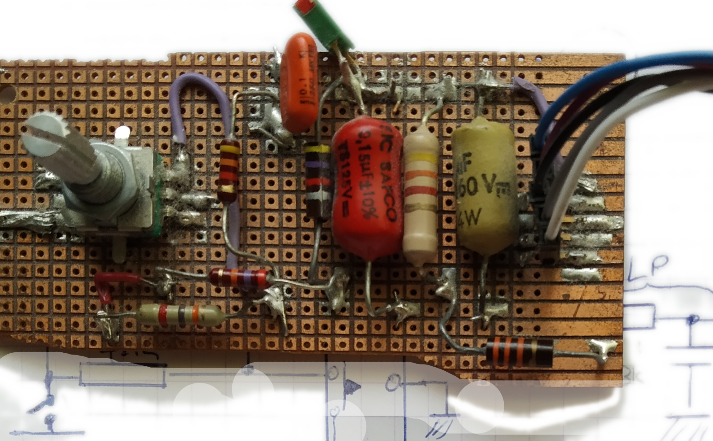
We connect the encoder to the GPIO A port. For PA0 & PA1, an alternate function AF1 allows to input PA0 and PA1 on the inputs of TIM2 (channel 1 and 2).
The encoder yellow wire is connected to the Nucleo Power 3,3 V on CN6. The encoder black wire is connected to the Nucleo Power Ground on CN9.
Scope channel 1 (yellow probe) is connected to the A encoder (blue). Scope channel 2 (pink probe) is connected to the B encoder (white).
Software
Configure PA0 & PA1 as alternate functions
GPIO mode
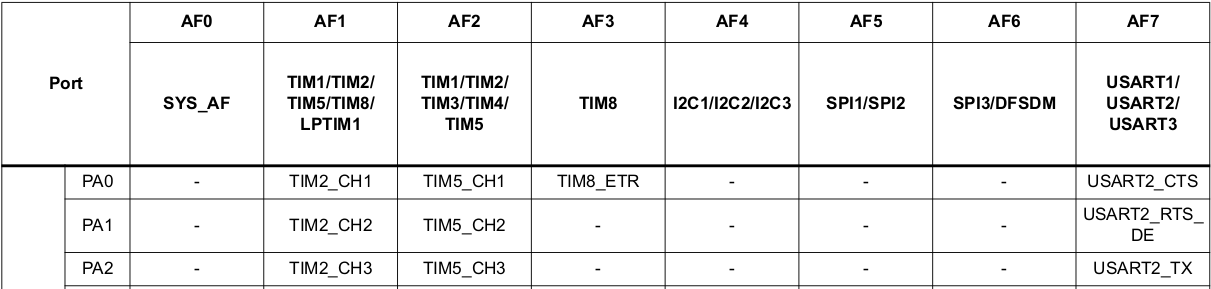
We have TIM2_CH1 (AF1) for PA0 and TIM2_CH2 (AF1) for PA1.
10: Alternate function mode
reset bit 0 with bic
set bit 1 with orr
// ----------- set PA0, PA1 alternate function
ldr r0, =GPIOA_BASE                //  4800 0000
ldr r1, [r0,#GPIO_MODER]
bic r1, r1, #GPIO_MODER_MODE0_0    // clear bit0 "x0"
orr r1, r1, #GPIO_MODER_MODE0_1    //   set bit1 "1x"
bic r1, r1, #GPIO_MODER_MODE1_0    // clear bit0 "x0"
orr r1, r1, #GPIO_MODER_MODE1_1    //   set bit1 "1x"
str r1, [r0,#GPIO_MODER]
GPIO Alternate function
Depending on the GPIO port number, we initialize either GPIOx_AFRL for GPIO pin 0 to 7, either GPIOx_AFRH for GPIO pin 8 to 15.
Since the GPIO port number is less than 7, we use the GPIOx_AFRL register.
For GPIOA pin 0 and 1, we use AFSEL0[0:3] and AFSEL1[0:3] and write the value corresponding to AF1, that is the binary value 0001 (ie 1 as in AF1):
set bit 0 with orr
clear bit 1 with bic
clear bit 2 with bic
ckear bit 3 with bic
// alternate function to TIM2_CH1 and TIM2_CH2
ldr  r1, =GPIOA_BASE   //  4800 0000
ldr r2,[r1,#AFRL]
orr r2,r2, #GPIO_AFRL_AFSEL0_0     // set bit 0
bic r2,r2, #GPIO_AFRL_AFSEL0_1    // clear bit 1
bic r2,r2, #GPIO_AFRL_AFSEL0_2    // clear bit 2
bic r2,r2, #GPIO_AFRL_AFSEL0_3    // clear bit 3
orr r2,r2, #GPIO_AFRL_AFSEL1_0
bic r2,r2, #GPIO_AFRL_AFSEL1_1
bic r2,r2, #GPIO_AFRL_AFSEL1_2
bic r2,r2, #GPIO_AFRL_AFSEL1_3
str r2,[r1,#AFRL]
select Encoder Interface mode
channel input stage

Let’s choose the following configuration:
CC1S= 01 (TIMx_CCMR1 register, TI1FP1 mapped on TI1)
CC2S= 01 (TIMx_CCMR1 register, TI2FP2 mapped on TI2)
TIMx_CCMR1 register
TIM2->CCMR1 |= (TIM_CCMR1_CC1S_0 | TIM_CCMR1_CC2S_0 );
We define the direction of the channel (input/output) and the used input.
Bits 1:0 CC1S[1:0]: Capture/Compare 1 selection
Bits 9:8 CC2S[1:0]: Capture/Compare 2 selection

01: CC1 channel is configured as input, IC1 is mapped on TI1.
01: CC2 channel is configured as input, IC2 is mapped on TI2.
Note that the Input capture filters (ICxF digital filters) are off, the sampling is done at fDTS.
TIMx_CCER register
capture/compare enable register
Select the TI1 and TI2 polarity by programming bit 1 CC1P and bit 5 CC2P in the TIMx_CCER register. In fact, we keep the reset values.
CC1P= ‘0’, CC1NP = ‘0’, IC1F =’0000’ (TI1FP1 noninverted, TI1FP1 = TI1)
CC2P= ‘0’, CC2NP = ‘0’, IC2F =’0000’ (TI2FP2 noninverted, TI2FP2=TI2)
0: OC1 active high (output mode) / Edge sensitivity selection (input mode)
When CC1 channel is configured as input, both CC1NP/CC1P bits select the active polarity of TI1FP1 and TI2FP1 for trigger or capture operations.
CC1NP=0, CC1P=0: non-inverted/rising edge. The circuit is sensitive to TIxFP1 rising edge, TIxFP1 is not inverted (trigger operation in gated mode or encoder mode).
TIMx_SMCR register
TIMx slave mode control register
We tell the TIM to operate in encoder mode as following
Bits 16, 2, 1, 0 SMS[3:0]: slave mode selection
When external signals are selected, the active edge of the trigger signal (TRGI) is linked to the polarity selected on the external input.
0011: Encoder mode 3 - Counter counts up/down on both TI1FP1 and TI2FP2 edges depending on the level of the other input.
TIM2->SMCR |= TIM_SMCR_SMS_0 | TIM_SMCR_SMS_1; SMS= ‘011’: both inputs are active on both rising and falling edges
TIMx_CR1 register
Depending on the sequence the counter counts up or down, the DIR bit in the TIMx_CR1 register is modified by hardware accordingly.
The DIR bit is calculated at each transition on any input (TI1 or TI2), whatever the counter is counting on TI1 only, TI2 only or both TI1 and TI2.
Behavior
The counter is clocked by each valid transition on TI1FP1 or TI2FP2 (TI1 and TI2 after input filter and polarity selection, TI1FP1=TI1 if not filtered and not inverted, TI2FP2=TI2 if not filtered and not inverted) assuming that it is enabled (CEN bit in TIMx_CR1 register written to ‘1).
The sequence of transitions of the two inputs is evaluated and generates count pulses as well as the direction signal.
Encoder interface mode acts simply as an external clock with direction selection. This means that the counter just counts continuously between 0 and the auto-reload value in the TIMx_ARR register (0 to ARR or ARR down to 0 depending on the direction).
So the TIMx_ARR must be configured before starting. In the same way, the capture, compare, prescaler, trigger output features continue to work as normal.
In this mode, the counter is modified automatically following the speed and the direction of the quadrature encoder and its content, therefore, always represents the encoder’s position.
The count direction correspond to the rotation direction of the connected sensor. The table summarizes the possible combinations, assuming TI1 and TI2 do not switch at the same time.
Enable counter
•CEN= 1 (TIMx_CR1 register, Counter is enabled)
One-pulse mode (OPM)
The one-pulse mode (OPM) is used together with the timer channels configured in output mode.
It allows the timer to generate a pulse of a programmable width after a programmable delay on the timer channels configured in PWM1 or PWM2 output compare modes.
This mode is activated by setting the OPM bit in the TIMx_CR1 timer register.
Each time that the OPM control bit is set, and a timer update event occurs, the timer counter enable control bit (CEN) is reset and the counter is frozen to its value at the update event.
If the timer update event is masked by some means, the one-pulse operating mechanism is unable to reset the CEN control-bit and the timer counter keeps running.
The timer’s outputs continue to output their configured waveforms.
A possibility to mask the effect of a timer update event is to set the UDIS control bit.
Another way to mask the timer update event is by making the timer repetition counter register’s content different from zero.
Not all the STM32 timer peripherals embed the repetition counter.
Given the previous condition, and considering that each time that the update event occurs (with masked effect), the repetition counter content is decremented, then, this behavior can be used to generate a series of pulses.
For instance, to generate a series of 5 pulses, the repetition counter should be set to 4.
The first four updated events are masked as the repetition counter content is different from zero.
These four first update events do not reset the CEN control bit but they decrement the repetition counter content down to zero. The fifth update event is the one that resets the CEN control (the repetition counter is already at zero).
This way, the timer counter has overflowed five times before being disabled and the five required pulses are generated.
With default channel output polarity, the PWM2 output mode gives the typical pulse waveform, like a delay for a given time, then a pulse with given duration.
For inversed polarity, either the channel output polarity should be inversed or the PWM1 output mode should be used.
The outputted waveform is characterized by two parameters: the pulse and the delay lengths
Generate a series of pulses
Set the OPM bit in the TIMx_CR1 timer register to activate the OPM mode.
To obtain N pulse at the output, put (N-1) into the TIMx_RCR register.
The repetition counter registers is found in General purpose timers 15, 16 and 17, and also in advanced timers.
The architecture of TIM 15 is as:

TIM16 and TIM17 have a simpler architecture:

Note that TIM15 has two Capture/Compare registers, so we choose it. In TIM15, there is also a SMCR register (offset 0x08).
We configure TIM15_CH1 as an output called E, via for example GPIOA PA2 and connect it to a scope.

schematics (C05 board)

As we can see, the Nucleo terminal PA2 (on header CN9) is not connected to the pin 16 of the MCU (PA2 output) via SB63.
Instead of closing SF63 with solder, we can use others ports PB14, PF9 or PG10. We use PB14 and connect it to an oscilloscope:

To connect PB14 to the channel 1 output of TIM15, we use its alternate function AF14.

// enable GPIO port B clock
RCC->AHB2ENR |= RCC_AHB2ENR_GPIOBEN;

// set PB14 as alternate function mode "10"
GPIOB->MODER &= ~GPIO_MODER_MODE14_0;
GPIOB->MODER |=  GPIO_MODER_MODE14_1;

// connect timer15 CH1 output -> PB14 via alternate function AF14  "1110"

// use AFR[1]/AFRH as GPIO pin 14 > 0..7
GPIOB->AFR[1] &= ~(GPIO_AFRH_AFSEL14_0);
GPIOB->AFR[1]= GPIO_AFRH_AFSEL14_1 | GPIO_AFRH_AFSEL14_2 | GPIO_AFRH_AFSEL14_3;
For GPIOB pin 14, we use AFSEL14[0:3] and write the value corresponding to AF14, that is the binary value 1110 (ie 14 as in AF14).
We want the signal E to be as follows:

E is 1 for 15 us
E is 0 for 45 us
Everytime counter ARR overflows or underflows, the repetition counter RCR is decremented by 1.
In one pulse mode (OPM), when the repetition counter reaches 0, it is reloaded and an update event happens.
Timer clock
APB2 peripheral clock enable register (RCC_APB2ENR)

// --- enable GP timer 15 clock ---
RCC->APB2ENR |= RCC_APB2ENR_TIM15EN;
Capture and compare
We use the second Capture/compare register CCR2 for comparison (we’ll need CCR1 for DMA).
CCMR1 register
Specific to General-purpose timers (TIM15/TIM16/TIM17):

Notice that there is no Output Compare clear enable bit (OC1CE, OC2CE).
Channel circuit

// ------ CCMR1 register ------------------
// "00": CC1 channel is configured as output

TIM15->CCMR1 |=  TIM_CCMR1_OC2PE; // Output Compare 2 preload enable
TIM15->CCMR1 &= ~TIM_CCMR1_CC2S_0; // "00": CC2 channel is configured as output
TIM15->CCMR1 &= ~TIM_CCMR1_CC2S_1; // "00": CC2 channel is configured as output
Output stage of capture/compare channel (channel 1)

// OC1M[3:0]: Output compare 1 mode
// 0111: PWM mode 2
// 0110: PWM mode 1
TIM15->CCMR1 &= ~TIM_CCMR1_OC2M_0;
TIM15->CCMR1 |=  TIM_CCMR1_OC2M_1;
TIM15->CCMR1 |=  TIM_CCMR1_OC2M_2;

// ------------ CCER register ------------------
TIM15->CCER &= ~TIM_CCER_CC2P; // OC2 active high (output mode)
TIM15->CCER |=  TIM_CCER_CC2E; // Capture mode enabled
// OC2 signal is output on the corresponding output pin

// ----- break and dead-time register BDTR register  -------------
TIM15->BDTR |=  TIM_BDTR_MOE;
DMA request
Timer DMA-burst configuration
We want to change the period (ARR) and the pulse length (CMR1) of the waveform.
The TIM2 timer DMA-burst should be configured as below:
•As there are three timer registers to update, the burst transfer length is 3. The DBL[4:0] control bit-field within the TIM1_DCR should be set to 2. Three data transferred each UEV, three update event occur. •Among the timer registers to update, the timer TIM1_ARR register is the first in the TIM1 timer register map, so it is defined as the base for the transfer. The DBA[4:0] control bit-filed should be set in order to point to the TIM1_ARR register (DBA[4:0] = 11). .. figure:: ../img/DMA.png
- width:
520px
- alt:
DMA mapping
We use the ****first Capture/compare register CCR1 for DMA.
DMA/interrupt enable register (DIER) for TIM16 and TIM17:

for TIM15

AHB1 peripheral clock enable register (RCC_AHB1ENR)

TIM15->DIER |=  TIM_DIER_CC1DE;  // in CC1 DMA enable
RCC->AHB1ENR |= RCC_AHB1ENR_DMA1EN;
The hardware requests from the peripheral TIM 15 is mapped to the DMA channel through the DMA_CSELR channel selection register.

For TIM15, we have to use channel5 for DMA1.
Each channel has a channel peripheral address register (CPAR).
DMA channel peripheral address register (DMA_CPARx) Address offset: 0x10 + 0x14 * (x - 1), (x = 1 to 7)

Here, the direction of the transfer is from memory to peripheral.
CPAR is the destination register that contains the base address of the peripheral data register to which the data is written.
Each channel has a channel memory address register (CMAR).
DMA channel x memory address register (DMA_CMARx) Address offset: 0x14 + 0x14 * (x - 1), (x = 1 to 7)

CMAR is the source register ta=hat contains the base address of the memory from which the data is read.
DMA1_Channel5->CPAR = (uint32_t)&GPIOA->BSRR;    // address of bit set/reset register
DMA1_Channel5->CMAR = (uint32_t)BSRR; // memory address register
BSRR bit set/reset register
DMA channel x configuration register (DMA_CCRx)
Address offset: 0x08 + 0x14 * (x - 1), (x = 1 to 7)

MEM2MEM: we disable memory to memory mode (“0”)
- PL[1:0]: Priority level
Here low priority “00”
MSIZE[1:0]: Memory size
Here defines the data size of the array that DMA reads. “10” for 32 bits.
PSIZE[1:0]: Peripheral size
Here defines the data size of the peripheral into which DMA writes. “10” for 32 bits.
When we send data from memory to a peripheral, we usually want to write an aera of memory to the same peripheral address.
MINC: Memory increment mode 1: increment mode enabled
PINC: Peripheral increment mode 0: disable
CIRC: Circular mode disabled
DIR: Data transfer direction
1: Read from memory
The 3 following flags era disabled:
TEIE: Transfer error interrupt enable HTIE: Half transfer interrupt enable TCIE: Transfer complete interrupt enable
DMA channel number of data to transfer register (DMA_CNDTRx)

General purpose timers (2)
General purpose TIMER
Let’s use TIM2 channel 1, 2, 3 and 4.

With alternate functions AF1, we get PA0, PA1, PA2 and PA3:

For PA0 and PA1, we can use A0 and A1 of CN8:

// ---- timer 2 ----------------------
// set PA0 as alternate function "10"
GPIOB->MODER &= ~GPIO_MODER_MODE0_0;  // x0
GPIOB->MODER |=  GPIO_MODER_MODE0_1;  // 1x

// connect timer2 CH1 output -> PA0 via alternate function AF1  "0001"
GPIOB->AFR[0] |=   GPIO_AFRL_AFSEL0_0 ;
GPIOB->AFR[0] &= ~(GPIO_AFRL_AFSEL0_1);
GPIOB->AFR[0] &= ~(GPIO_AFRL_AFSEL0_2);
GPIOB->AFR[0] &= ~(GPIO_AFRL_AFSEL0_3);
Timer configuration with registers
TIMx control register 1 (TIMx_CR1)(x = 2 to 5)
CMS[1:0]: Center-aligned mode selection 00: Edge-aligned mode. The counter counts up or down depending on the direction bit (DIR).
DIR: Direction 0: counter used as upcounter
We clear CMS (2 bits mask=11) and DIR:
TIM1->CR1 &= ~(TIM_CR1_DIR | TIM_CR1_CMS);
CKD[1:0]: Clock division This bit-field indicates the division ratio between the timer clock (CK_INT) frequency and sampling clock used by the digital filters (ETR, TIx),
00: tDTS = tCK_INT <—— 01: tDTS = 2 × tCK_INT 10: tDTS = 4 × tCK_INT
TIM1->CR1 &= ~(TIM_CR1_CKD);
TIM2->PSC = 48000-1; // prescaler  48 MHz x 1 ms -1 = 47999
TIM2->ARR = period-1;
TIM2->CCR1 = nb_pulses;  // pulse compare value

// ---------- RCR Repetition register ----------
TIM2->RCR = nb_pulses - 1;
There is no repetition counter (RCR) in timers 2, 3, 4 and 5. Only TIM1, TIM8, TIM15, TIM16 and TIM17.
TIMx event generation register (TIMx_EGR)(x = 16, 17)

BG: Break generation
COMG: Capture/Compare control update generation
CC1G: Capture/Compare 1 generation
UG: Update generation
**TIMx event generation register (TIM15_EGR)

It has two more control bits: TG & CC2G:
BG: Break generation
TG: Trigger generation
COMG: Capture/Compare control update generation
CC2G: Capture/Compare 2 generation
CC1G: Capture/Compare 1 generation
UG: Update generation
TIMx event generation register (TIMx_EGR)(x = 2 to 5)

TG: Trigger generation
CC4G: Capture/compare 4 generation
CC3G: Capture/compare 3 generation
CC2G: Capture/compare 2 generation
CC1G: Capture/compare 1 generation
UG: Update generation
TIM1->EGR = TIM_EGR_UG; /* Generate an update event to reload the Prescaler
TIM15 slave mode control register (TIM15_SMCR)

no slave mode control register for GP timers TIM16 & TIM17
TIMx slave mode control register (TIMx_SMCR)(x = 2 to 5)
TIM2->SMCR = 0; // reset
TIMx control register 1 (TIMx_CR1)(x = 2 to 5)
TIM2->CR1 |= TIM_CR1_OPM; // one pulse mode
TIMx capture/compare mode register 1 (TIMx_CCMR1)(x = 2 to 5)
OC1M[3:0]: Output compare 1 mode
0111: PWM mode 2 - In upcounting, channel 1 is inactive as long as TIMx_CNT<TIMx_CCR1, else active.

TIM2->CCMR1 |=  TIM_CCMR1_OC1M_0;
TIM2->CCMR1 |=  TIM_CCMR1_OC1M_1;
TIM2->CCMR1 |=  TIM_CCMR1_OC1M_2;
TIM2->CCMR1 &= ~TIM_CCMR1_OC1M_3;  // x0111   PWM2
Capture/Compare channel main circuit
CC1S * “00”: CC1 channel is configured as output
TIM2->CCMR1 &= (uint16_t)~TIM_CCMR1_CC1S;
TIMx capture/compare enable register (TIMx_CCER)(x = 2 to 5)
CC1P: Capture/Compare 1 output Polarity.
0: OC1 active high (output mode) / Edge sensitivity selection (input mode, see below)

CCxP does not define an absolute polarity. It simply switches on an inverter between OCxREFC signal and the output pin (use of inverter when 1).
For GP TIM2, TIM3, TIM4 & TIM5, there is no Break and dead-time (BDTR) and no repetition counter (RCR) registers.
TIM2->BDTR |= TIM_BDTR_MOE; /* Enable the TIM main Output */
TIM2->CR1 |= TIM_CR1_CEN; /* Enable the TIM peripheral */
PWM mode 1 and mode 2
0110: PWM mode 1
In upcounting, channel 1 is active as long as TIMx_CNT<TIMx_CCR1, else inactive. In downcounting, channel 1 is inactive (OC1REF=‘0) as long as TIMx_CNT>TIMx_CCR1 else active (OC1REF=1).
0111: PWM mode 2
In upcounting, channel 1 is inactive as long as TIMx_CNT<TIMx_CCR1 else active. In downcounting, channel 1 is active as long as TIMx_CNT>TIMx_CCR1 else inactive.

*signals active high (CC1P & CC2P=0) *in yellow, PWM mode 1 *in purple, PWM mode 2
// 0110: PWM mode 1
TIM2->CCMR1 &= ~TIM_CCMR1_OC1M_0;
TIM2->CCMR1 |=  TIM_CCMR1_OC1M_1;
TIM2->CCMR1 |=  TIM_CCMR1_OC1M_2;
TIM2->CCMR1 &= ~TIM_CCMR1_OC1M_3;

// 0111: PWM mode 2
TIM2->CCMR1 |=  TIM_CCMR1_OC2M_0;
TIM2->CCMR1 |=  TIM_CCMR1_OC2M_1;
TIM2->CCMR1 |=  TIM_CCMR1_OC2M_2;
TIM2->CCMR1 &= ~TIM_CCMR1_OC2M_3;

Phase signals - Quadrature signals
The possible master/slave connections are given in:
TIMx internal trigger connection


Three timers will be cascaded:
TIM1 MASTER

TRIGGER OUTPUT parameters:
MSM (Master Slave mode): disabled
Trigger event selection TRGO:
TIMx control register 2 (TIMx_CR2)(x = 1, 8)
MMS[2:0]: Master mode selection These bits allow selected information to be sent in master mode to slave timers for synchronization (TRGO). 101: Compare - OC2REFC signal is used as trigger output (TRGO)
MMS2[3:0]: Master mode selection 2 These bits allow the information to be sent to ADC for synchronization (TRGO2) to be selected. The combination is as follows: 0000: Reset -
Advanced timers
The STM32L476 offers two advanced 16-bit timers.
Advanced timers
One pulse mode OPM
extern void init_timer(void)
{
    period = 120;
    pulse= 100;

// ----- enable advanced timer 1 clock --------
RCC->APB2ENR |= RCC_APB2ENR_TIM1EN;

TIM1->PSC =  48-1;   // prescaler  48 MHz x 1 us -1 = 47  unity= 1 us
TIM1->ARR =  120-1;  // period-1
TIM1->CCR1 = 100;   // time before pulse
TIM1->RCR = 2-1;

// ------------- one pulse mode ------------------
TIM1->CR1 |= TIM_CR1_OPM;

// ----------------- CCMR1 register ------------------
TIM1->CCMR1 |=  TIM_CCMR1_OC1PE; // Output Compare 1 preload enable
TIM1->CCMR1 &= ~TIM_CCMR1_CC1S_0; // "00": CC1 channel is configured as output
TIM1->CCMR1 &= ~TIM_CCMR1_CC1S_1; // "00": CC1 channel is configured as output

/* --------------- select PWM ---------------- */
// 0111: PWM mode 2
TIM1->CCMR1 |=  TIM_CCMR1_OC1M_0;
TIM1->CCMR1 |=  TIM_CCMR1_OC1M_1;
TIM1->CCMR1 |=  TIM_CCMR1_OC1M_2;
TIM1->CCMR1 &= ~TIM_CCMR1_OC1M_3;

// ----------------- CCER register ------------------
TIM1->CCER &= ~TIM_CCER_CC1P;  // Output Compare Polarity OC1 active high (output mode)
TIM1->CCER |=  TIM_CCER_CC1E; // enable the Capture output channel 1 mode

// ----- break and dead-time register BDTR register -------------
TIM1->BDTR |= TIM_BDTR_MOE; // enable the TIM main output
}
extern void init_gpio(void)
{
// ----------- enable GPIO port A B C clocks -------------
RCC->AHB2ENR |= RCC_AHB2ENR_GPIOAEN;

// set PA8 as alternate function "10"
GPIOA->MODER &= ~GPIO_MODER_MODE8_0;
GPIOA->MODER |=  GPIO_MODER_MODE8_1;

// connect timer1 CH1 output -> PA8 via alternate function AF1  "0001"
GPIOA->AFR[1] |=   GPIO_AFRH_AFSEL8_0 ;
GPIOA->AFR[1] &= ~(GPIO_AFRH_AFSEL8_1);
GPIOA->AFR[1] &= ~(GPIO_AFRH_AFSEL8_2);
GPIOA->AFR[1] &= ~(GPIO_AFRH_AFSEL8_3);
}
#include "stm32l476xx.h"

extern void init_clock(void)
{

// -------- put LATENCY before changing MSI frequency ------------------

// Bit 8 PRFTEN: Prefetch enable
FLASH->ACR = FLASH_ACR_LATENCY_2WS | FLASH_ACR_PRFTEN;

// -------- choose MSI frequency ------------------
RCC->CR &= ~RCC_CR_MSIRANGE;
RCC->CR = RCC_CR_MSIRGSEL | RCC_CR_MSIRANGE_11 ;   // 48 MHz
// RCC->CR = RCC_CR_MSIRGSEL | RCC_CR_MSIRANGE_0;   // 400 kHZ

}
Master/ slave synchronisation
We want to generate the following signal:

Four pulses of 20 us width are generated at a period 1/F2 of 4 ms.
- We use two timers:
- - advanced timer TIM1 as a slave timer in one pulse mode (OPM)- general purpose timer TIM2 as a master timer configured to trig TIM1
With a system frequency of 48 MHz, the master timer TIM2 is configured as:
// ********* TIMER 2 MASTER *************
TIM2->PSC =  48-1;    // prescaler  48 MHz x 1 us-1 = 47  unity= 1 us
TIM2->ARR =  4000-1;  // 4 ms repetition period
The slave timer is configured in 4-pulse mode (OPM with a repetition of 3) and PWM mode 2:
// ********* TIMER 1 ***********
TIM1->PSC =  48-1;      // prescaler  48 MHz x 1 us -1 = 47  unity= 1 us
TIM1->ARR =  period-1;  // period-1
TIM1->CCR1 = pulse;     // waiting time before pulse
TIM1->RCR =  4-1;

// Update Request Source: only overflow/underflow
// OPM : One Pulse Mode (fire once)
TIM1->CR1 = 0x00; //reset
TIM1->CR1 |= TIM_CR1_URS | TIM_CR1_OPM;
TIM1->CR1 |= TIM_CR1_OPM;

// ----------------- CCMR1 register ------------------
TIM1->CCMR1 |=  TIM_CCMR1_OC1PE; // Output Compare 1 preload enable
TIM1->CCMR1 &= ~TIM_CCMR1_CC1S_0; // "00": CC1 channel is configured as output
TIM1->CCMR1 &= ~TIM_CCMR1_CC1S_1; // "00": CC1 channel is configured as output

/* --------------- select the PWM mode */
// OC1M[3:0]: Output compare 1 mode
// 0111: PWM mode 2
// 0110: PWM mode 1
TIM1->CCMR1 |=  TIM_CCMR1_OC1M_0;
TIM1->CCMR1 |=  TIM_CCMR1_OC1M_1;
TIM1->CCMR1 |=  TIM_CCMR1_OC1M_2;
TIM1->CCMR1 &= ~TIM_CCMR1_OC1M_3;

// ----------------- CCER register ------------------
TIM1->CCER &= ~TIM_CCER_CC1P;  // Output Compare Polarity OC1 active high (output mode)
TIM1->CCER |=  TIM_CCER_CC1E; // enable the Capture output channel 1 mode
The two timers are connected in the following way:

How do we connect TIM2 Trigger Output (TRGO) to TIM1 Internal trigger (ITR1) ?
MASTER configuration
The TIM2 master timer is configured in master trigger mode with its internal TRGO signal used to trigger TIM1 (via ITR1) at every update event.
This is done through “Master mode selection” (MMS) = 010 “Update” in the Control register #2.
TIMx control register 2 (TIMx_CR2)(x = 1, 8)

// ********* TIMER 2 MASTER *************
// 010: Update (trigger output TRGO)
TIM2->CR2 &= ~TIM_CR2_MMS_0;
TIM2->CR2 |=  TIM_CR2_MMS_1;
TIM2->CR2 &= ~TIM_CR2_MMS_2;
SLAVE configuration
Advanced-control timer block diagram
Two steps are necessary.
step 1
First, be aware that only a few timers can be master of TIM1, as shown below:
For the slave TIM1, the multiplexer TS (Trigger Selection) allows to select between four master timers (TIM15, TIM2, TIM3 and TIM4) to forward the selected input to the Slave mode selection (SMS).
With the master TIM2, we must select Internal Trigger ITR1.
0110: Trigger Mode - The counter starts at a rising edge of the trigger TRGI
TIMx slave mode control register (TIMx_SMCR)(x = 1, 8)
/******* Slave mode configuration *********/
// Select the TIM_TS_ITR1 signal as Input trigger for the timer
// 001: Internal Trigger 1 (ITR1)
TIM1->SMCR |=  TIM_SMCR_TS_0;
TIM1->SMCR &= ~TIM_SMCR_TS_1;
TIM1->SMCR &= ~TIM_SMCR_TS_2;
step 2
** SMS[3:0]: Slave mode selection**
Choose
0111: External Clock Mode 1 - Rising edges of the selected trigger (TRGI) clock the counter
or
1000: Combined reset + trigger mode
// 0110: Trigger Mode - The counter starts at a rising edge of the trigger TRGI
// 0110 SMS slave mode selection
TIM1->SMCR &= ~TIM_SMCR_SMS_0;
TIM1->SMCR |=  TIM_SMCR_SMS_1;
TIM1->SMCR |=  TIM_SMCR_SMS_2;
TIM1->SMCR &= ~TIM_SMCR_SMS_3;
Here the result with 2 channels, the first one is in PWM2 mode and the second in PWM1:


Master controls several slaves in parallel
The possible master/slave connections are given in:
TIMx internal trigger connection
Therefore, the choice of timers will depend on the available trigger connections.
example

0001: Set channel 1 to active level on match. OC1REF signal is forced high when the counter TIMx_CNT matches the capture/compare register 1 (TIMx_CCR1).