GPIO
GPIO stands for General Purpose Input/Output.

Let’s choose a GPIO port pin, available on the Nucloe L476 – for example, PA6 on CN10/CN5, pin 13. Connect an LED to this pin and to GND, with a 220 ohms resistor (or a greater value).

Note
PA13, PA14, PA15 - PB3 and PB4 are normally used for debugging purposes

GPIO configuration
Configuration of GPIO pins is achieved by configuring the GPIO registers (12 different registers):


Every port, from port A to port I, has a distinct base address, eg “0x4800 0000” for GPIOA, “0x4800 0400” for GPIOB, etc.
To access in assembler a specific register of a specific GPIO module, use the base address and add an offset:
ldr  r1, =GPIOA_BASE           // 0x4800 0000
ldr  r2, [r1,#GPIO_BSSR]               // read at base address plus offset (0x18)
Clock Configuration
Most periphery clocks are disabled by default to save power.
In order to turn on the GPIOA module to which the desired pin PA6 belongs, the bit IOPAEN must be set to 1.
AHB2 peripheral clock enable register (RCC_AHB2ENR)

Since this is the first bit (number zero), a value of 0x0000 0001 must be written in the register.
The AHB2ENR address is at offset 0x4c from the RCC register address (4002 1000). To access RCC_AHB2ENR, we want to access the location pointed to by 0x40021000 + 0x4c.
We use RCC_AHB2ENR_GPIOAEN, with following definitions:
#define RCC_AHB2ENR_GPIOAEN_Pos    (0U)
#define RCC_AHB2ENR_GPIOAEN_Msk    (0x1UL << RCC_AHB2ENR_GPIOAEN_Pos)  // 0000 0001
#define RCC_AHB2ENR_GPIOAEN         RCC_AHB2ENR_GPIOAEN_Msk
One way to activate the GPIOA clock, without changing the others bits of the AHB2ENR RCC register, is the following:
ldr  r1, =RCC_BASE       //  4002 1000
ldr  r2, [r1,#AHB2ENR]   //  4002 104c
orr  r2, #RCC_AHB2ENR_GPIOAEN   // enable GPIO port A  #0x01
str  r2, [r1,#AHB2ENR]
There is no problem with r2 (RCC_AHB2ENR) containing 1s, since the reset has cleared all the RCC_AHB2ENR bits. If r2 contains several ones, the OR operator would not change anything.
RCC->AHB2ENR |= RCC_AHB2ENR_GPIOAEN;
Mode configuration
It is made through the MODE register

Address offset:0x00 Reset value: 0xABFF FFFF (for port A) Reset value: 0xFFFF FEBF (for port B)
On STM32L47x/L48x: Reset value: 0xFFFF FFFF (for ports C..G) Reset value: 0x0000 000F (for port H)
There are sixteen 2-bit MODE available, corresponding to I/O pin #0 to #15. For PA6, we need to use MODE6.
GPIO_MODER_MODE6_Pos   =      (12U)
GPIO_MODER_MODE6_Msk   =      (0x3UL << GPIO_MODER_MODE6_Pos)         /*!< 0x00003000 */
GPIO_MODER_MODE6       =       GPIO_MODER_MODE6_Msk
GPIO_MODER_MODE6_0     =      (0x1UL << GPIO_MODER_MODE6_Pos)         /*!< 0x00001000 */
GPIO_MODER_MODE6_1     =      (0x2UL << GPIO_MODER_MODE6_Pos)         /*!< 0x00002000 */

/* Legacy defines */
#define GPIO_MODER_MODER6                   GPIO_MODER_MODE6
#define GPIO_MODER_MODER6_0                 GPIO_MODER_MODE6_0
#define GPIO_MODER_MODER6_1                 GPIO_MODER_MODE6_1
00: Input mode
01: General purpose output mode                GPIO_MODER_MODEx_0
10: Alternate function mode            GPIO_MODER_MODEx_1
11: Analog mode (reset state)
With libopencm 3
#define GPIO_MODE_INPUT                 0x00    /* default */
#define GPIO_MODE_OUTPUT                0x01
#define GPIO_MODE_AF                    0x02
#define GPIO_MODE_ANALOG                0x03
Output mode configuration

The output mode offers two options:
Push-pull output mode
Open-drain output mode
The mode is activated through GPIO port pull-up / pull-down register (GPIOx_PUPDR).
GPIO port output type register (GPIOx_OTYPER)(x = A to I)
The control is done through the GPIO port output type register (GPIOx_OTYPER).

0: Output push-pull (reset state) 1: Output open-drain

Address offset: 0x08 Reset value: 0x0C00 0000 (for port A) Reset value: 0x0000 0000 (for the other ports)
00: Low speed
01: Medium speed
10: High speed
11: Very high speed
GPIO port pull-up/pull-down register (GPIOx_PUPDR)(x = A to I).

Address offset: 0x0C Reset value: 0x6400 0000 (for port A) Reset value: 0x0000 0100 (for port B) Reset value: 0x0000 0000 (for other ports)
00: No pull-up, pull-down
01: Pull-up
10: Pull-down
11: Reserved
GPIO port output data register (GPIOx_ODR)(x = A to I).
Writing the related bit of the output register (GPIOx_ODR) to 0 forces the I/O pin to ground. Writing the related bit of the output register (GPIOx_ODR) to 1 forces the I/O pin to VDD.

Address offset: 0x14 Reset value: 0x0000 0000
GPIO port bit set/reset register (GPIOx_BSRR) (x = A to I)</h3>

Address offset: 0x18 Reset value: 0x0000 0000
Input mode configuration

5V tolerant inputs
“Up to 114 fast I/Os, most 5 V-tolerant, up to 14 I/Os with independent supply down to 1.08 V.”
When applying a voltage you should be aware to limit it for some GPIO, as shown below:
5 V tolerant I/O pin (FT):
3.6 V tolerant I/O pin (TT):
source: datasheet table #16
Input options
The input mode offers three options:
Connect a button
In the Nucleo L476, there is a blue button connected to PC13.

When the button is pressed, the GPIO PC13, thet must be configured as input, becomes low.
// configure PC13 as input
ldr r1, =GPIOC_BASE
ldr r2,[r1,#GPIO_MODER]
bic r2, #GPIO_MODER_MODE13_0   // reset bit 0 mode 13 -> "x0"
bic r2, #GPIO_MODER_MODE13_1   // reset bit 1 mode 13 -> "0x"
str r2,[r1,#GPIO_MODER]
// configure PC13 as input
GPIOC->MODER &=  GPIO_MODER_MODE13_0;   // input mode "00"
GPIOC->MODER &= ~GPIO_MODER_MODE13_1;
Note
    //  check bit 13 of IDR register
if ((GPIOC->IDR & GPIO_IDR_ID13) == GPIO_IDR_ID13)
{
            // if button pressed, do something
}
If the button is connected to GPIO in this way

it is necessary to configure the GPIO input in pull-up.
When the button is pressed, the PA1 voltage will go to zero.
We need to modify the GPIOx_PUPDR Register for GPIO A1
//   input PA1 - button
GPIOC->MODER &=  GPIO_MODER_MODE1_0;   // input mode "00"
GPIOC->MODER &= ~GPIO_MODER_MODE1_1;

// pull-up output "01" because the button connects to ground
GPIOA->PUPDR |=  GPIO_PUPDR_PUPD1_0;
GPIOA->PUPDR &= ~GPIO_PUPDR_PUPD1_1;
Read GPIO inputs
GPIO port input data register (GPIOx_IDR) (x = A to I)
Address offset: 0x10
Reset value: 0x0000 XXXX

The 16 bits of the register contain the input value of the corresponding I/O port.
(gdb) x 0x48000810
0x48000810: 0x00002000 // blue button not pressed

(gdb) x 0x48000810
0x48000810: 0x00000000 // blue button pressed
bit 13 set
15 14 13 12   11 10 9 8   7 6 5 4  3 2 1 0
0  0  1  0    0  0  0 0   0 0 0 0  0 0 0 0        -> hex 2000
Alternate functions
Several functions, such as timers, communication functions (SPI, UART, I2C, etc) are available.
For Port B, we have:

Note
You can find tables for alternate functions AF0 to AF7 and AF8 to AF15 for ports A to H in the L476 datasheet.
We set the alternate mode of the GPIO pin x by setting the bit 1 and resetting the bit 0:
For example, for PB9:
// ----------- set PB9 alternate function
ldr  r1, =GPIOB_BASE                //  4800 0400
ldr  r2, [r1,#GPIO_MODER]
bic r2, r2, #GPIO_MODER_MODE9_0     // clear mode9 bit "x0"
orr r2, r2, #GPIO_MODER_MODE9_1     //   set mode9 bit "1x"
str  r2, [r1,#GPIO_MODER]


Since the pin number is greater than 7, we use the GPIOx_AFRH register
// alternate function to I2C1   AFRH->AFSEL[8] =  AF4
ldr  r1, =GPIOB_BASE   //  4800 0400
ldr r2,[r1,#AFRH]
bic r2,r2, #GPIO_AFRH_AFSEL8_0
bic r2,r2, #GPIO_AFRH_AFSEL8_1
orr r2,r2, #GPIO_AFRH_AFSEL8_2
bic r2,r2, #GPIO_AFRH_AFSEL8_3
str r2,[r1,#AFRH]
// set open-drain
ldr  r1, =GPIOB_BASE
ldr  r2, [r1,#OTYPER]
bic  r2, #GPIO_OTYPER_OT8   // 1: output open drain
bic  r2, #GPIO_OTYPER_OT9   // 1: output open drain
str  r2, [r1,#OTYPER]
// set pin speed
ldr  r2, [r1,#OSPEEDR]
orr  r2,r2, #GPIO_OSPEEDR_OSPEED8_0
orr  r2,r2, #GPIO_OSPEEDR_OSPEED8_1
str  r2, [r1,#OSPEEDR]
//  00: No pull-up, pull-down   01: Pull-up   10: Pull-down
ldr  r2, [r1,#PUPDR]
bic  r2, #GPIO_PUPDR_PUPD6_1   // pull-up 0x
orr  r2, #GPIO_PUPDR_PUPD6_0   // pull-up x1
str  r2, [r1,#PUPDR]
Analog configuration
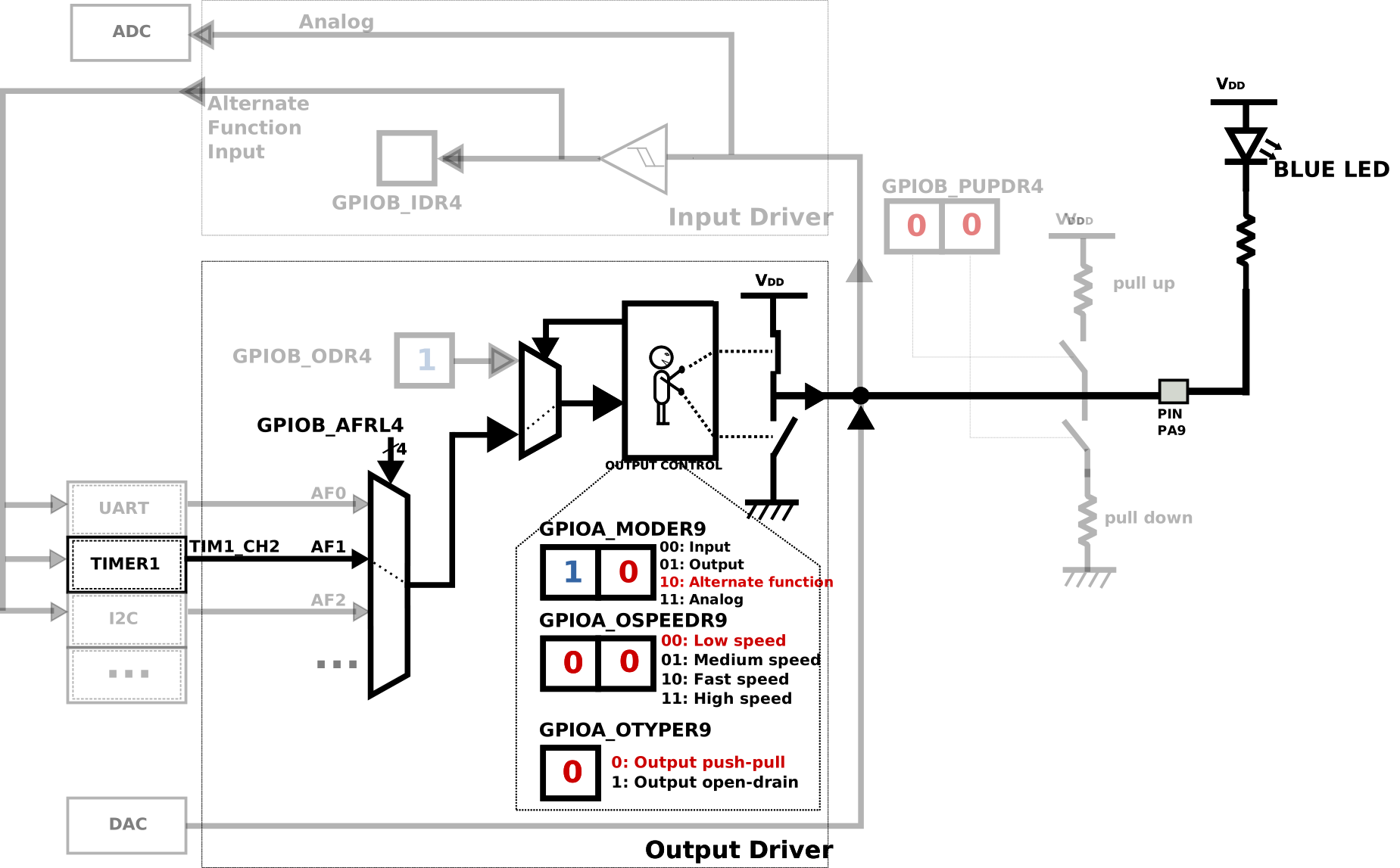
Some GPIO pins can be configured in analog mode which allows the use of ADC, DAC, OPAMP, and COMP internal peripherals.
To use a GPIO pin in analog mode, the following register are considered:
Blink LED GPIO assembler program
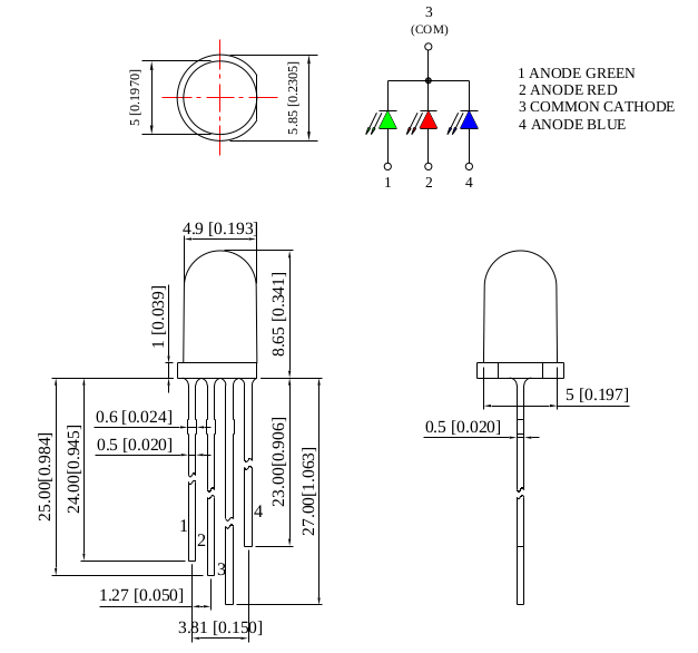
A tricolor LED is connected to PA6 (2 red), PA7 (4 blue), PB6 (1 green) and Nucleo ground (3 COM). The 3,3 V from CN8 Nucleo is also used.
Assembler program
 1.syntax unified
 2.cpu cortex-m4
 3.arch armv7e-m
 4.thumb
 5
 6// =======================================================
 7// .section .VectorTable, "a"   // a allocable
 8.word 0x20000400         // stack end
 9// .word 0x80000ed		 // main - address 0x04 Reset_Handler
10// .word _StackEnd
11// .word Reset_Handler + 1
12.word Reset_Handler
13.space 0xf8
14
15// =======================
16//  peripheral memory map
17.include "gpio.inc"
18// =======================
19
20.text
21
22.type Reset_Handler, %function
23//.thumb_func   // the following is instructions, not data. Thus lsbit of address is set.
24Reset_Handler:
25// enable the GPIOA clock via the AHB2ENR register
26ldr  r1, =RCC_BASE       //  4002 1000
27ldr  r2, [r1,#AHB2ENR]   //  4002 104c
28orr  r2, #RCC_AHB2ENR_GPIOAEN
29orr  r2, #RCC_AHB2ENR_GPIOBEN
30str  r2, [r1,#AHB2ENR]
31
32ldr  r1, =GPIOA_BASE        //  4800 0000
33ldr  r2, [r1,#GPIO_MODER] 	// after reset, r2 is 0xabffffff
34bic  r2, #GPIO_MODER_MODE6_1     // reset bit 1 mode 6  -> "01"    set PA6 to OUTPUT mode  2*6=12
35bic  r2, #GPIO_MODER_MODE7_1     // reset bit 1 mode 7  -> "01"    set PA6 to OUTPUT mode  2*7=14
36str  r2, [r1,#GPIO_MODER]
37
38ldr  r1, =GPIOB_BASE        //  4800 0400
39ldr  r2, [r1,#GPIO_MODER] 	// after reset, r2 is 0xabffffff
40bic  r2, #GPIO_MODER_MODE6_1     // reset bit 1 mode 6  -> "01"    set PA6 to OUTPUT mode  2*6=12
41str  r2, [r1,#GPIO_MODER]
42
43// set PUSH-PULL/open-drain mode
44ldr  r1, =GPIOA_BASE        //  4800 0000
45ldr  r2, [r1,#GPIO_OTYPER] 	// after reset, r2 is 0xabffffff
46bic  r2, #GPIO_OTYPER_OT6	 // 0: output push-pull (reset state)
47bic  r2, #GPIO_OTYPER_OT7	 // 0: output push-pull (reset state)
48str	 r2, [r1,#GPIO_OTYPER]	//  value of PA OTYPE register
49
50// set pin speed
51ldr  r1, =GPIOA_BASE        //  4800 0000
52ldr  r0, [r1,#GPIO_OSPEEDR]	//  value of PA OSPEED register
53ldr  r2, = GPIO_OSPEEDR_OSPEED6_0
54ldr  r3, = GPIO_OSPEEDR_OSPEED6_1   //  10
55orr  r0, r0, r2
56orr  r0, r0, r3
57str	 r0, [r1,#GPIO_OSPEEDR]
58
59// set "no pull"
60//  00: No pull-up, pull-down   01: Pull-up   10: Pull-down  11: Reserved
61ldr  r1, =GPIOA_BASE        //  4800 0000
62ldr  r2, [r1,#GPIO_PUPDR]	//  value of PUPD register
63bic  r2, #GPIO_PUPDR_PUPD6_0	 // no pull (reset state)
64str	 r2, [r1,#GPIO_PUPDR]
65
66// ---------------------------------------------------------------
67ldr r3, =4000000
68ldr r5, =2000000
69
70ldr  r1, =GPIOA_BASE        //  4800 0000
71ldr  r2, [r1,#GPIO_BSRR]
72orr  r2, #GPIO_BSRR_BS_6	// PA6 red led
73orr  r2, #GPIO_BSRR_BS_7	// PA7 blue led
74str	 r2, [r1,#GPIO_BSRR]
75
76mov r4, r3
77delay0: subs r4, #1
78bne delay0
79
80
81ldr r1, =GPIOB_BASE			//  4800 0400
82ldr r6, =GPIO_BSRR_BR_6
83ldr r7, =GPIO_BSRR_BS_6
84
85BlinkLoop:					// blink green led, blue and red stay lighted
86str	r7, [r1,#GPIO_BSRR]
87
88mov r4, r5
89delay1: subs r4, #1
90bne delay1
91
92str	r6,	[r1,#GPIO_BSRR]
93
94mov r4, r3
95delay2: subs r4, #1
96bne delay2
97
98b BlinkLoop