Direct Memory Address - DMA
Presentation
Direct memory access (DMA) is a peripheral that is used to quickly move data between peripherals and memory, as well as memory to memory, without any CPU action.
Here is the STM32L4x bus matrix:

It is not clear whether DMAs can or cannot move data from the I-bus to I-code.

The matrix manages the access arbitration between masters, which are shown on top. The Cortex-M4 core and the two DMA controllers communicate with the bus slaves, shown on the right.
The matrix is composed of five masters (CPU AHB, system bus, DCode bus, ICode bus, DMA1 and DMA2) and six slaves (FLASH, SRAM1, SRAM2, AHB1 (including APB1 & APB2), AHB2, FMC external/QUADSPI).
Let’s consider master DMA1. When we trace a vertical line, we see six (or seven) dots which connect to a slave.
The two DMA masters can access all memories and peripherals.
With the STM32L476, the two DMA controllers have each 7 channels. Each channel has an arbiter for handling the priority between DMA requests.
The priority of each channel is configured in the DMA_CCRx register.
There are four different levels of priority:
very high
high
medium
low
There are 7 channels for DMA1 (and 7 for DMA2). This accounts for 7 DMA channel registers necessary for channel configuration (DMA_CCR1 to DMA_CCR7), channel peripheral address (DMA_CPAR1 to DMA_CPAR7), channel memory address (DMA_CMAR1 to DMA_CMAR7), etc.
However, these registers are called differently: DMA1_Channel5->CCR, instead of DMA1_CCR5 for example.

DMA memory-to-memory transfer
Lets create a simple DMA memory-to-memory transfer from RAM to RAM.
Configure DMA as follows:
DMA CCR
DMA channel x configuration register (DMA_CCRx)

For every channel ‘x’, register DMA_CCRx (DMA1_Channelx->CCR) has a memory-to-memory mode (MEM2MEM) bit control.
In this mode, the DMA channels operate without being triggered by a request from a peripheral.
If the MEM2MEM bit in the DMA_CCRx register is set, the channel, if enabled, initiates transfers. The transfer stops once the DMA_CNDTRx register reaches zero.

Configure the channel priority using the PL[1:0] bits in the DMA1_Channelx->CCR register. Configure also data transfer direction, circular mode, peripheral & memory incremented mode, peripheral & memory data size, and -if required- interrupt after half and/or full transfer in the same register.
CPAR
Set the peripheral address register in the DMA_CPARx register. The data will be moved from/ to this address to/ from the memory after the peripheral event.
DMA channel peripheral address register (DMA_CPARx)

CPAR is the destination register that contains the base address of the peripheral data register to which the data is written.
CMAR
Each channel has a channel memory address register (CMAR).
DMA channel x memory address register (DMA_CMARx)

CMAR is the source register that contains the base address of the memory from which the data is read.
Set the memory address in the DMA_CMARx register. The data will be written to or read from this memory after the peripheral event.
CNDTR
DMA channel number of data to transfer register (DMA_CNDTRx)

Configure the total number of data to be transferred in the DMA_CNDTRx register. After each peripheral event, this value will be decremented.
Create two global buffers: the first as a source data, and the second as a destination buffer.
const uint8_t Buffer_Src[]={0,1,2,3,4,5,6,7,8,9};  // if not const, garbage
uint8_t Buffer_Dest[10];
Configure and activate DMA:
DMA1_Channel5->CCR = 0;   // clear DMA1->CCR5
DMA1_Channel5->CCR |= DMA_CCR_MEM2MEM;

// set DMA source and destination addresses.
// source: address of the buffer in memory.
DMA1_Channel5->CMAR  = (uint32_t)&Buffer_Src;   // byte -> 32-bit register
// destination
DMA1_Channel5->CPAR  = (uint32_t)&Buffer_Dest;  // DAC1->DHR12R1
// set DMA data transfer length
DMA1_Channel5->CNDTR = (uint32_t)10;

DMA1_Channel5->CCR &= ~DMA_CCR_MSIZE_0;   // "x0"  32 bits memory
DMA1_Channel5->CCR |=  DMA_CCR_MSIZE_1;   // "1x"  32 bits memory
DMA1_Channel5->CCR &= ~DMA_CCR_PSIZE_0;   // "x0"  32 bits memory
DMA1_Channel5->CCR |=  DMA_CCR_PSIZE_1;   // "1x"  32 bits memory
DMA1_Channel5->CCR |= DMA_CCR_MINC;       // memory increment mode
DMA1_Channel5->CCR |= DMA_CCR_PINC;
DMA1_Channel5->CCR |= DMA_CCR_DIR;        // read from memory

DMA1_Channel5->CCR |= DMA_CCR_EN;  // activate the channel
DMA errors
How do we know if the DMA transfer was made without error ?
If there is a transfer error, the channel is automatically disabled by hardware (DMA_CCR_EN=0 for the channel).
Check also the TEIF, HTIE and TCIE bits in the DMA interrupt status register (DMA_ISR).
|TEIFx: Transfer error (TE) interrupt flag for channel x |HTIFx: Half transfer (HT) interrupt flag for channel x |TCIFx: Transfer complete (TC) interrupt flag for channel x |GIFx: Global interrupt flag for channel x
There is no need to enable the corresponding interrupts in the DMA_CCRx register:
|TEIE: Transfer error interrupt enable |HTIE: Half transfer interrupt enable |TCIE: Transfer complete interrupt enable
If the destination buffer width is less than the source buffer width, errors will occur.
uint8_t Buffer_Dest[4];
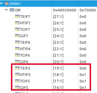
For channel 5, we see that there is no transfer error TE (the first 4 bytes were correctly transmitted). But there is a HT (Half transfer) error since only 4 out of 10 bytes were transfered. Thus, the transfer is not complete (TC error) and the GIF (Global interrupt flag) is also set.
DMA memory-to-peripheral transfer
In the memory-to-memory mode (MEM2MEM set), the DMA channel operate without being triggered by a request from a peripheral.
In the memory-to-peripheral mode, the DMA channel needs to be triggered by a request from a peripheral, for example TIM2.
DMA channel selection register (DMA_CSELR)

The hardware requests from the TIM2 peripheral are mapped to the DMA channels through the DMA_CSELR channel selection register:

We need to write the 4 bits ‘0b0100’ in C5S connecting channel5 and TIM2_CH1:

TIMER
TIM2->DIER = TIM_DIER_CC1DE_Msk; // enable timer channel 1 DMA request (goes to DMA channel 5)
// TIM2->EGR = TIM_EGR_CC1G_Msk; // channel 1 can generate events - not used

// ----- break and dead-time register BDTR register -------------
TIM2->BDTR |= TIM_BDTR_MOE; // enable the TIM main output

TIM2->CR1 |= TIM_CR1_ARPE; // preload switched on
TIM2->CR1 |= TIM_CR1_CEN;
DMA
RCC->AHB1ENR |= RCC_AHB1ENR_DMA1EN;  // DMA1 clock enable

// set DMA source and destination addresses.
// source: address of the buffer in memory.
DMA1_Channel5->CMAR = (uint32_t)&Buffer_CCR1;   // source -> memory address register
DMA1_Channel5->CPAR  = (uint32_t)&TIM2->CCR1;
// set DMA data transfer length
DMA1_Channel5->CNDTR = (uint32_t)110;

DMA1_Channel5->CCR &= ~DMA_CCR_MSIZE_0;   // "x0"  32 bits memory
DMA1_Channel5->CCR |=  DMA_CCR_MSIZE_1;   // "1x"  32 bits memory
DMA1_Channel5->CCR &= ~DMA_CCR_PSIZE_0;   // "x0"  32 bits memory
DMA1_Channel5->CCR |=  DMA_CCR_PSIZE_1;   // "1x"  32 bits memory

DMA1_Channel5->CCR |= DMA_CCR_MINC;     // memory increment mode
// PINC Peripheral increment mode is disabled -> DMA always writes into the same register
DMA1_Channel5->CCR &= ~DMA_CCR_PINC;     // peripheral increment mode

DMA1_Channel5->CCR |= DMA_CCR_CIRC; // circular mode
DMA1_Channel5->CCR |= DMA_CCR_DIR;  // read from memory

DMA1_Channel5->CCR |= DMA_CCR_EN;

// TIM2_CH1 triggers DMA1 channel 5
// C5S[3:0]: DMA channel 5 selection
DMA1_CSELR->CSELR |= (0b0100 << DMA_CSELR_C5S_Pos);
TIMx control register 2 (TIMx_CR2)(x = 2 to 5)

In order to make the timer work with the DMA, we need to configure CCDS: Capture/compare DMA selection in Control Register 2 (CR2).
CCDS: Capture/compare DMA selection 0: CCx DMA request sent when CCx event occurs 1: CCx DMA requests sent when update event occurs
DMA channel x configuration register (DMA_CCRx)
MEM2MEM: let’s disable memory to memory mode (“0”)
- PL[1:0]: Priority level
Choose low priority “00”
MSIZE[1:0]: Memory size
Let’s define the data size of the array that DMA will read. “10” for 32 bits.
PSIZE[1:0]: Peripheral size
And the data size of the peripheral into which DMA will write. “10” for 32 bits.
When we send data from memory to a peripheral, we usually want to write a group of a number of memory contents into the same peripheral address.
MINC: Memory increment mode 1: increment mode enabled
PINC: Peripheral increment mode 0: disable
CIRC: Circular mode disabled
DIR: Data transfer direction
1: Read from memory
The 3 following flags era disabled:
TEIE: Transfer error interrupt enable HTIE: Half transfer interrupt enable TCIE: Transfer complete interrupt enable
The peripheral TIM2 channel sends a single DMA request signal to the DMA controller.

We see that channel 5 is associated with timer 2 channel 1.
Timer DMA-burst configuration
*We want to change the period (ARR) and the pulse length (CMR1) of the waveform.
*Since there are two timer registers to update, the burst transfer length is 2.
The DMA base address (DBA[4:0]) is a 5 bits control field that defines the base-address for DMA transfers (when read/write access are done through the TIMx_DMAR address).
DBA is defined as an offset starting from the address of the TIMx_CR1 register.
TIMx DMA control register (TIMx_DCR)(x = 2 to 5)

Among the timer registers to update, the timer TIM2_ARR register is the first in the TIM2 timer register map, so it is defined as the base for the transfer.
The DBA[4:0] control bit-filed should be set in order to point to the TIM1_ARR register (DBA[4:0] = 11).
/* Reset DBA and DBL bit fields */
TIM2->DCR &= ~TIM_DCR_DBA;
TIM2->DCR &= ~TIM_DCR_DBL;
/* Select the DMA base register and DMA burst length */
TIM2->DCR = TIM_DMABase_ARR | TIM_DMABurstLength_3Transfers;
- alt:
DMA mapping
We use the ****first Capture/compare register CCR1 for DMA.
DMA/interrupt enable register (DIER) for TIM16 and TIM17:

for TIM15

AHB1 peripheral clock enable register (RCC_AHB1ENR)

TIM15->DIER |=  TIM_DIER_CC1DE;  // in CC1 DMA enable
RCC->AHB1ENR |= RCC_AHB1ENR_DMA1EN;
The hardware requests from the peripheral TIM 2is mapped to the DMA channel through the DMA_CSELR channel selection register.

For TIM2, we have to use channel5 for DMA1.
Each channel has a channel peripheral address register (CPAR).
DMA channel peripheral address register (DMA_CPARx) Address offset: 0x10 + 0x14 * (x - 1), (x = 1 to 7)
Here, the direction of the transfer is from memory to peripheral.
CPAR is the destination register that contains the base address of the peripheral data register to which the data is written.
Each channel has a channel memory address register (CMAR).
DMA channel x memory address register (DMA_CMARx) Address offset: 0x14 + 0x14 * (x - 1), (x = 1 to 7)
CMAR is the source register that contains the base address of the memory from which the data is read.
DMA1_Channel5->CPAR = (uint32_t)&GPIOA->BSRR;    // address of bit set/reset register
DMA1_Channel5->CMAR = (uint32_t)BSRR; // memory address register
BSRR bit set/reset register
DMA channel number of data to transfer register (DMA_CNDTRx)
Yes; in this context, it’s the DMA request (trigger) coming from TIM6’s Update event, if enabled by setting TIM6_DIER.UDE.
> as somehow distinct from the timer trigger-output TRGO?
TRGO is output of the multiplexer controlled by TIMx_CR2.MMS. If TIMx_CR2.MMS is set to 0b010, TRGO is identical to Update, but otherwise it’s not.
> Second, what does it mean to have two sources listed for the same mux setting?
ST’s documentation is not great in those details. They are probably just ORed together, so…
> Does the notation “TIM6_UP DAC_CH1” mean that either source can trigger the DMA transfer, and the user is responsible for ensuring that only one of them actually does?
… yes.
> I’ll note that in the STM32L4* HAL manual (UM1884), chapter 22 allows the DMA_InitTypeDef::Request field to take the value of DMA_REQUEST_DAC1_CH1 or DMA_REQUEST_TIM6_UP – which seems to imply that these are different values.